 ChipApex | Global Electronic Components Supplier
SEARCH
Search Product
Search Post
— IC芯片 | 连接器 | 传感器 | 被动器件 —
Search productSearch post
— IC芯片 | 连接器 | 传感器 | 被动器件 —
Consult the customer manager about the wholesale price.
consultation hotline:86-132-6715-2157
email:[email protected]
Contact the product manager for consultation. One-stop consultation is available.
Do you want a lower wholesale price? Please send us your inquiry and we will reply immediately.
The AT17F080A-30JI is an 8-Mbit serial configuration memory device designed for Field Programmable Gate Arrays (FPGAs). It operates at a maximum clock frequency of 10 MHz with a supply voltage range of 2.97 V to 3.63 V. The component utilizes a low-power CMOS Flash process and features 5V tolerant I/O pins. It supports In-System Programming (ISP) via a 2-wire bus and offers a typical endurance of 5,000 write cycles. The device is housed in a 20-lead PLCC package and functions within an industrial temperature range of -40°C to +85°C.
Verify the specific ordering suffix 'JI' corresponds to the Industrial temperature range (-40°C to +85°C) and the 20-lead PLCC package as defined in the manufacturer's ordering guide. Confirm that the source documentation explicitly lists this exact part number variant before finalizing procurement specifications.
Select this component when designing systems requiring non-volatile storage for FPGA configuration data. Ensure the target FPGA supports Master Serial mode compatibility. Verify that the system design accommodates the 20-lead PLCC footprint and that the operating environment remains within the specified industrial temperature limits.
This device belongs to the AT17FxxxA series of In-System Programmable Configuration PROMs. These configurators are engineered to provide cost-effective memory solutions for loading configuration programs into programmable logic devices. The series supports both commercial and industrial temperature grades across various package options.
The AT17F080A-30JC serves as a functional substitute within the same series, offering identical electrical characteristics but restricted to the commercial temperature range (0°C to 70°C).
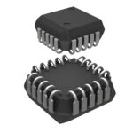 AT17F080A-30JI
The activity of extra discounts on wholesale prices is in full swing…
Please fill in your contact information and we will send you the latest wholesale price list.





