 ChipApex | Global Electronic Components Supplier

SEARCH
Search Product
Search Post
— IC芯片 | 连接器 | 传感器 | 被动器件 —
Search productSearch post
— IC芯片 | 连接器 | 传感器 | 被动器件 —
Consult the customer manager about the wholesale price.
consultation hotline:86-132-6715-2157
email:[email protected]
Contact the product manager for consultation. One-stop consultation is available.
Do you want a lower wholesale price? Please send us your inquiry and we will reply immediately.
AT24C1024B-PU25 is listed in the Memory IC range at ChipApex. The manufacturer field lists Microchip Technology. Its product description is IC EEPROM 1MBIT I2C 1MHZ 8DIP. Review the specifications below when checking this part for your BOM.
The AT24C1024B-PU25 is a 1,048,576-bit (131,072 x 8) serial electrically erasable and programmable read-only memory (EEPROM). It operates within a supply voltage range of 2.5V to 5.5V and supports I²C clock frequencies up to 1 MHz at these voltages. The device features a 256-byte page write mode, hardware and software data protection via the WP pin, and an industrial temperature range of –40°C to +85°C. It is housed in an 8-lead PDIP package.
Verify the ordering suffix 'PU25' corresponds to the bulk form only variant in the 8-lead PDIP package. Confirm the specific voltage code matches the required operating range of 2.5V to 5.5V. Ensure the component meets the specified industrial temperature requirements for the target application environment.
Select this part when a large non-volatile memory capacity is needed alongside a standard I²C interface. The 2.5V voltage option provides compatibility with higher voltage logic levels while maintaining low standby current. Consider the page write capability for efficient data logging applications that require frequent updates.
This component belongs to the AT24Cxx family of serial EEPROMs manufactured by Microchip Technology. It shares architectural similarities with other members like the AT24C256 but offers significantly higher density. The device utilizes a self-timed write cycle mechanism typical of CMOS EEPROM technology.
Direct replacements include other AT24C1024B variants with different packages or voltage codes, such as AT24C1024B-PU for 1.8V operation. Cross-family equivalents may exist but require verification of pinout and electrical specifications.
When a page write sequence reaches the end of the 256-byte page, the internal address rolls over to the beginning of the same page. Subsequent bytes overwrite existing data within that page rather than advancing to the next page.
The A1 and A2 pins serve as device address inputs that allow up to four devices to be addressed on a single I²C bus. They can be hardwired to VCC or GND to set unique addresses.
Explore related parts through Memory, Integrated Circuits (ICs), all product categories, ChipApex homepage.
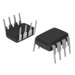 AT24C1024B-PU25

The activity of extra discounts on wholesale prices is in full swing…
Please fill in your contact information and we will send you the latest wholesale price list.





