 ChipApex | Global Electronic Components Supplier

SEARCH
Search Product
Search Post
— IC芯片 | 连接器 | 传感器 | 被动器件 —
Search productSearch post
— IC芯片 | 连接器 | 传感器 | 被动器件 —
Consult the customer manager about the wholesale price.
consultation hotline:86-132-6715-2157
email:[email protected]
Contact the product manager for consultation. One-stop consultation is available.
Do you want a lower wholesale price? Please send us your inquiry and we will reply immediately.
AT49BV002-12JC is listed in the Memory IC range at ChipApex. The manufacturer field lists Microchip Technology. Its product description is IC FLASH 2MBIT PARALLEL 32PLCC. Review the specifications below when checking this part for your BOM.
The AT49BV002-12JC is a 2-megabit (256K x 8) parallel NOR Flash memory manufactured by Microchip Technology. It operates on a single 3-volt supply with an access time of 120 ns and active current consumption of 50 mA. The device features a sector architecture including a 16K-byte boot block, two 8K-byte parameter blocks, and two main memory blocks. It supports byte-by-byte programming and sector erase operations within the commercial temperature range of 0°C to 70°C.
Verify the specific ordering suffix 'JC' corresponds to the 32-lead PLCC package and commercial temperature range. Confirm that the 'BV' designation indicates the 2.7V to 3.6V operating voltage window. Ensure compatibility with existing system voltage levels and interface timing requirements before procurement.
Select this component when a 2-megabit capacity with a 120 ns access speed is required. The PLCC package is suitable for through-hole mounting or specific socketed applications. Consider the boot block lockout feature if system security is a priority. Verify that the parallel interface aligns with the host controller's memory bus capabilities.
This part belongs to the AT49BV/LV002 family of 3-volt Flash memories. It utilizes advanced CMOS technology for low power dissipation. The device is designed for in-system reprogramming, allowing updates without removal from the circuit board. It serves as a nonvolatile storage solution for microcontroller-based designs.
Check for AT49BV002-90JC for faster access times. AT49LV002-12JC offers a narrower voltage range. Verify pinout compatibility with alternative packages like TSOP or VSOP variants within the same memory density family.
The lockout is enabled by executing a specific six-command sequence to designated addresses. Once activated, the boot block cannot be erased or programmed with input voltages of 5.5V or less.
The RESET pin halts current device operations and places outputs in a high-impedance state when held low. Applying 12V to this pin can override the boot block lockout during erase or program cycles.
Explore related parts through Memory, Integrated Circuits (ICs), all product categories, ChipApex homepage.
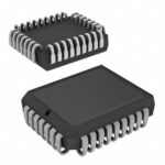 AT49BV002-12JC

The activity of extra discounts on wholesale prices is in full swing…
Please fill in your contact information and we will send you the latest wholesale price list.





