 ChipApex | Global Electronic Components Supplier
SEARCH
Search Product
Search Post
— IC芯片 | 连接器 | 传感器 | 被动器件 —
Search productSearch post
— IC芯片 | 连接器 | 传感器 | 被动器件 —
Consult the customer manager about the wholesale price.
consultation hotline:86-132-6715-2157
email:[email protected]
Contact the product manager for consultation. One-stop consultation is available.
Do you want a lower wholesale price? Please send us your inquiry and we will reply immediately.
The ATF16V8C-5JX is a high-performance Electrically-Erasable Programmable Logic Device (EE PLD) manufactured by Microchip Technology. It utilizes EECMOS Flash memory technology and features a maximum pin-to-pin propagation delay of 5 ns. The device operates within a commercial temperature range of 0°C to 70°C with a supply voltage of 5V ± 5%. It incorporates eight macrocells, each allocated eight product terms, and supports three operational modes: registered, complex, and simple. Key electrical characteristics include a standby current of up to 130 mA and a power-down mode current below 100 μA when controlled via Pin 4.
Verify that the specific design requires the power-down feature enabled on Pin 4; otherwise, the pin functions as a standard logic input. Confirm compatibility with existing JEDEC fuse files if the power-down option is not utilized in the logic design. Ensure programming equipment supports the extended feature set of the ATF16V8C series.
Select this component for designs requiring direct emulation of 20-pin PAL architectures with enhanced reprogrammability. Choose the -5 speed grade for applications demanding a maximum 5 ns delay. Verify that the operating environment remains within the commercial temperature range of 0°C to 70°C and the supply voltage stays within 5V ± 5%.
The ATF16V8C-5JX belongs to the ATF16V8C family of EE PLDs. It is housed in a 20-lead Plastic J-leaded Chip Carrier (PLCC) package, designated as package type 20J. This package conforms to JEDEC reference MS-018, Variation AA, and provides a standard pinout compatible with legacy 20-pin PLD footprints.
The ATF16V8C-5JX serves as a drop-in replacement for many 20-pin PALs. Specific emulated devices include the 16R8, 16RP8, 16R6, 16RP6, 16R4, and 16RP4 families when configured in registered mode. In complex mode, it can emulate 16L8, 16H8, and 16P8 devices.
The device includes internal input and I/O pin-keeper circuits that hold pins at their previous value, preventing them from floating to indeterminate levels without requiring external pull-up resistors.
Pin 4 can be configured as a power-down control pin. When high, it reduces total current consumption to less than 100 μA. If the power-down feature is not specified in the design file, Pin 4 functions as a standard logic input.
Registers reset to the low state slightly after VCC crosses the reset voltage (VRST). The VCC rise must be monotonic from below 0.7V, and all input/feedback setup times must be met before driving the clock term high.
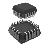 ATF16V8C-5JX
The activity of extra discounts on wholesale prices is in full swing…
Please fill in your contact information and we will send you the latest wholesale price list.





