 ChipApex | Global Electronic Components Supplier
ATTINY861A-SUR
Search Product
Search Post
— IC芯片 | 连接器 | 传感器 | 被动器件 —
Search productSearch post
— IC芯片 | 连接器 | 传感器 | 被动器件 —
Consult the customer manager about the wholesale price.
consultation hotline:86-132-6715-2157
email:[email protected]
Contact the product manager for consultation. One-stop consultation is available.
Do you want a lower wholesale price? Please send us your inquiry and we will reply immediately.
The ATTINY861A-SUR is an 8-bit AVR microcontroller featuring 8K bytes of In-System Programmable Flash, 512 bytes of EEPROM, and 512 bytes of SRAM. It operates at speeds up to 20 MHz with a throughput of 20 MIPS. The device supports a supply voltage range of 1.8V to 5.5V and includes 16 programmable I/O lines. Key peripherals include an 11-channel 10-bit ADC, an analog comparator, two timers/counters, and a Universal Serial Interface (USI). It utilizes a 32-pad MLF package.
Verify the specific speed grade suffix matches the required operating frequency and voltage range. Confirm the MLF package variant aligns with PCB footprint requirements. Ensure the ordering code corresponds to the correct memory size within the ATtinyx61A family. Check for RoHS compliance status if mandated by project specifications.
Select this component when 8K Flash and 512-byte RAM are required alongside extensive analog input channels. The MLF package suits compact surface-mount designs. Consider the 20 MHz maximum speed for processing-intensive tasks within the 1.8V to 5.5V operational window. Evaluate the USI interface compatibility against standard SPI or I2C master/slave needs.
This part belongs to the ATtinyx61A series, which shares architectural similarities with the ATtiny261A and ATtiny461A. The primary distinction lies in the memory capacities, where the 861A variant offers the highest storage within this specific group. All variants utilize the same enhanced RISC core and peripheral configuration.
ATtiny461A-SUR: Offers identical functionality with reduced memory capacity (4K Flash, 256B EEPROM/SRAM).
The center pad underneath the QFN/MLF package should be soldered to ground on the board to ensure mechanical stability.
AVCC should be externally connected to VCC even if some peripherals such as the ADC are not used.
The return address Program Counter is stored on the Stack, which is allocated in the general data SRAM. The Stack Pointer must be initialized by software before interrupts are enabled.
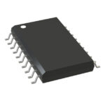 ATTINY861A-SUR
The activity of extra discounts on wholesale prices is in full swing…
Please fill in your contact information and we will send you the latest wholesale price list.





