 ChipApex | Global Electronic Components Supplier
SEARCH
Search Product
Search Post
— IC芯片 | 连接器 | 传感器 | 被动器件 —
Search productSearch post
— IC芯片 | 连接器 | 传感器 | 被动器件 —
Consult the customer manager about the wholesale price.
consultation hotline:86-132-6715-2157
email:[email protected]
Contact the product manager for consultation. One-stop consultation is available.
Do you want a lower wholesale price? Please send us your inquiry and we will reply immediately.
The AX8052F100-2-TA05 is an ultra-low power microcontroller in a QFN28 package, operating from 1.8 V to 3.6 V across -40°C to 85°C. It features a high-speed 8052-compatible core with 20 MIPS performance and 64 kBytes of FLASH memory offering 100,000 erase cycles. The device includes 8.25 kBytes of internal SRAM, three 16-bit general-purpose timers, two UARTs, a Master/Slave SPI controller, and a 10-bit 500 kSample/s ADC. Additional peripherals include analog comparators, a temperature sensor, a 2-channel DMA controller, and a dedicated AES crypto engine.
Verify the ordering suffix TA05 corresponds to the 500-unit tape and reel packaging format as specified in the official documentation. Confirm that the -2 speed grade variant meets the required operational frequency specifications for your design. Ensure the QFN28 thermal pad connection requirements are addressed in the PCB layout to maintain reliability within the specified temperature range.
Select this component when integrating with onsemi AXRadio ICs or similar SPI-based radio peripherals due to the dedicated Radio Master SPI interface. Consider the specific sleep mode current requirements to determine if the 256 Byte, 4 kByte, or 8 kByte RAM retention options suit the application's wake-up needs. Evaluate the need for the dedicated AES engine if cryptographic security is a primary design constraint.
This part belongs to the AX8052 family of ultra-low power microcontrollers designed primarily for battery-operated radio applications. It shares the same core architecture and peripheral set as other variants in the series, differing mainly in speed grades and packaging configurations. The device is optimized for low idle power consumption while maintaining high performance during active execution.
AX8052F100-3-TA05: Higher speed grade variant with identical pinout and functionality.
The debug interface uses a 3-wire protocol where one wire is dedicated (DBG_EN) and two wires (PB6, PB7) are shared with GPIO pins. When DBG_EN is driven high, these pins convert to debug interface functions.
The debug interface can be locked using a user-programmable 64-bit key. Unauthorized persons cannot read the firmware through the debug interface without this key, though secure erase can still be initiated.
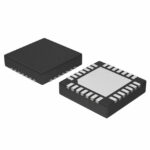 AX8052F100-2-TA05
The activity of extra discounts on wholesale prices is in full swing…
Please fill in your contact information and we will send you the latest wholesale price list.







