 ChipApex | Global Electronic Components Supplier
SEARCH
Search Product
Search Post
— IC芯片 | 连接器 | 传感器 | 被动器件 —
Search productSearch post
— IC芯片 | 连接器 | 传感器 | 被动器件 —
Consult the customer manager about the wholesale price.
consultation hotline:86-132-6715-2157
email:[email protected]
Contact the product manager for consultation. One-stop consultation is available.
Do you want a lower wholesale price? Please send us your inquiry and we will reply immediately.
The AZ23B5V6-HE3_A-08 is a silicon planar Zener diode array from the Vishay AZ23 series, housed in an SOT-23 package. It features a dual common-anode configuration with two independent Zener diodes sharing a single cathode connection. The nominal Zener voltage is 5.6 V with a tight tolerance of ±2%. It operates within a junction temperature range of -55 °C to +150 °C and dissipates up to 500 mW on lead clamping or 300 mW on an FR-4 board. The component is AEC-Q101 qualified for automotive applications.
Verify that the specific ordering code matches the required ±2% tolerance and AEC-Q101 qualification status. Confirm the package type is SOT-23 and check the manufacturer's latest datasheet revision for any updates to absolute maximum ratings or thermal characteristics before finalizing procurement specifications.
Select this component when a dual-channel Zener array with high precision is needed in a small form factor. Ensure the application current does not exceed the specified test currents (5 mA for low voltages, 2 mA for higher voltages). Verify that the operating ambient temperature remains within the -55 °C to +150 °C range to maintain performance integrity.
This part belongs to the Vishay AZ23 series of small signal Zener diodes. The series offers a wide range of standard E24 Zener voltages from 2.2 V to 75 V. Variants are available with ±5% or ±2% tolerances, and both commercial and AEC-Q101 qualified versions exist across different packaging options like SOT-23.
AZ23B5V6-E3-08: Commercial grade version without AEC-Q101 qualification.
The letter indicates the Zener voltage tolerance. 'C' denotes a standard ±5% tolerance, while 'B' specifies a tighter ±2% tolerance.
In this dual common-anode setup, the anodes of both Zener diodes are connected together internally. The cathodes serve as separate output terminals, allowing them to be used independently or in series/parallel configurations depending on the circuit design.
The device can dissipate up to 500 mW when leads are clamped between a recommended soldering footprint on an FR-4 board, or 300 mW under standard JEDEC testing conditions.
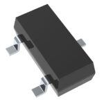 AZ23B5V6-HE3_A-08
The activity of extra discounts on wholesale prices is in full swing…
Please fill in your contact information and we will send you the latest wholesale price list.




