 ChipApex | Global Electronic Components Supplier
SEARCH
Search Product
Search Post
— IC芯片 | 连接器 | 传感器 | 被动器件 —
Search productSearch post
— IC芯片 | 连接器 | 传感器 | 被动器件 —
Consult the customer manager about the wholesale price.
consultation hotline:86-132-6715-2157
email:[email protected]
Contact the product manager for consultation. One-stop consultation is available.
Do you want a lower wholesale price? Please send us your inquiry and we will reply immediately.
The BCV61B,235 is an NPN general-purpose double transistor housed in a SOT143B surface-mounted plastic package. It features matched pairs with a DC current gain (hFE) range of 200 to 450 at VCE=5V and IC=2mA. The device supports a maximum collector current of 100 mA and peak currents of 200 mA. Voltage ratings include 30 V for both collector-base (VCBO) and collector-emitter (VCEO), with an emitter-base voltage limit of 6 V. Total power dissipation is rated at 250 mW at 25 °C ambient temperature.
Verify the specific ordering suffix matches the required production origin and packaging configuration. Confirm that the hFE binning aligns with circuit requirements, as the BCV61B variant specifies a gain range of 200 to 450. Ensure compatibility with SOT143B footprint dimensions during PCB layout verification.
Select this component when precise current matching between two NPN transistors is required within a single package. The BCV61B offers a mid-range current gain compared to other variants in the BCV61 family. Consider the thermal resistance characteristics and total power dissipation limits when designing for high ambient temperatures or dense board layouts.
This part belongs to the Nexperia BCV61 series of NPN general-purpose double transistors. It serves as the matched pair counterpart to the PNP BCV62 series. The device is designed for low-power analog and digital applications where space efficiency and parameter matching are critical design constraints.
The BCV62B is the direct PNP complement within the same package and feature set. Other BCV61 variants (BCV61A, BCV61C) share the package but differ in current gain specifications.
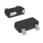 BCV61B,235
The activity of extra discounts on wholesale prices is in full swing…
Please fill in your contact information and we will send you the latest wholesale price list.





