 ChipApex | Global Electronic Components Supplier
SEARCH
Search Product
Search Post
— IC芯片 | 连接器 | 传感器 | 被动器件 —
Search productSearch post
— IC芯片 | 连接器 | 传感器 | 被动器件 —
Consult the customer manager about the wholesale price.
consultation hotline:86-132-6715-2157
email:[email protected]
Contact the product manager for consultation. One-stop consultation is available.
Do you want a lower wholesale price? Please send us your inquiry and we will reply immediately.
The BCV63B,215 is an NPN general-purpose double transistor housed in a small SOT143B Surface-Mounted Device plastic package. It features low current handling with a maximum collector current of 100 mA and low voltage ratings, including a maximum collector-emitter voltage of 30 V for Transistor TR1 and 6 V for Transistor TR2. The device is AEC-Q101 qualified for automotive applications. For the BCV63B variant, the DC current gain (hFE) ranges from 200 to 450 at specific test conditions. Total power dissipation is rated at 250 mW at 25 °C ambient temperature.
Verify the ordering code matches the required suffix for packing quantity. Confirm the marking code corresponds to the specific device variant. Check the product status on the manufacturer website as it may change. Ensure the application environment stays within the absolute maximum rating limits. Validate compatibility with the intended PCB footprint and soldering process.
Select this component when matched NPN transistors are required for precise circuit behavior. Consider the hFE range of 200-450 for the BCV63B variant during design. Ensure the operating voltage does not exceed the 30 V limit for TR1 or 6 V for TR2. Verify thermal management capabilities given the 250 mW power dissipation rating. Confirm suitability for the target manufacturing process.
This part belongs to the Nexperia BCV63 series of NPN general-purpose double transistors. It serves as the matched pair complement to the PNP BCV64B. The series is designed for compact designs requiring dual transistors with consistent electrical characteristics between the two dies within the single package.
BCV63 is the standard variant within the same package family.
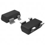 BCV63B,215
The activity of extra discounts on wholesale prices is in full swing…
Please fill in your contact information and we will send you the latest wholesale price list.





