ChipApex | Global Electronic Components Supplier
SEARCH
Search Product
Search Post
— IC芯片 | 连接器 | 传感器 | 被动器件 —
Search productSearch post
— IC芯片 | 连接器 | 传感器 | 被动器件 —
Consult the customer manager about the wholesale price.
consultation hotline:86-132-6715-2157
email:[email protected]
Contact the product manager for consultation. One-stop consultation is available.
Do you want a lower wholesale price? Please send us your inquiry and we will reply immediately.
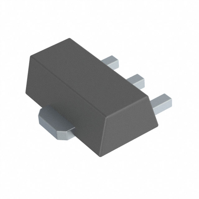
The BCX52-16,115 is a PNP medium power transistor from the BCX52 series, manufactured by Nexperia. It is housed in a SOT89 (SC-62) surface-mount plastic package with an exposed die pad for thermal management. The device supports a collector-emitter voltage of -60 V and a continuous collector current of -1 A. It features three DC current gain selections; the -16 suffix denotes a range of 100 to 250 at IC = -150 mA. Key electrical parameters include a peak collector current of -2 A, a transition frequency of 145 MHz, and a maximum power dissipation of 1.35 W on a 6 cm² copper pad. It is qualified to AEC-Q101 standards.
Verify the specific ordering code suffix matches the required hFE binning, as the -16 designation indicates a gain range of 100-250. Confirm the package type is SOT89 and check for RoHS compliance status. Ensure the procurement channel provides official Nexperia documentation to validate the component's authenticity and automotive qualification status before integration into production designs.
Select this component when a PNP medium power transistor with high current handling and robust thermal performance is required. The exposed pad design necessitates proper PCB copper area allocation to achieve specified power dissipation ratings. Consider the -16 gain bin if precise base drive control within the 100-250 range is critical for the amplifier or switching application.
This part belongs to the BCX52 family of 60 V, 1 A PNP transistors. It serves as the PNP complement to the BCX55 NPN series. The BCX52 variant specifically utilizes the SOT89 package, distinguishing it from the BCP52 (SOT223) and BC52PA (SOT1061) variants within the same product data sheet.
BCX55-16,115 (NPN complement)
The -16 suffix specifies the DC current gain (hFE) selection group, which ranges from 100 to 250 when measured at IC = -150 mA and VCE = -2V.
Yes, the BCX52 series is qualified in accordance with the AEC-Q101 standard for stress test qualification of discrete semiconductors.
The SOT89 package includes an exposed die pad that allows for excellent thermal and electrical conductivity when soldered to a sufficient copper area on the PCB.
 BCX52-16,115
The activity of extra discounts on wholesale prices is in full swing…
Please fill in your contact information and we will send you the latest wholesale price list.