ChipApex | Global Electronic Components Supplier
BD14231FVJ-CE2
Search Product
Search Post
— IC芯片 | 连接器 | 传感器 | 被动器件 —
Search productSearch post
— IC芯片 | 连接器 | 传感器 | 被动器件 —
Consult the customer manager about the wholesale price.
consultation hotline:86-132-6715-2157
email:[email protected]
Contact the product manager for consultation. One-stop consultation is available.
Do you want a lower wholesale price? Please send us your inquiry and we will reply immediately.
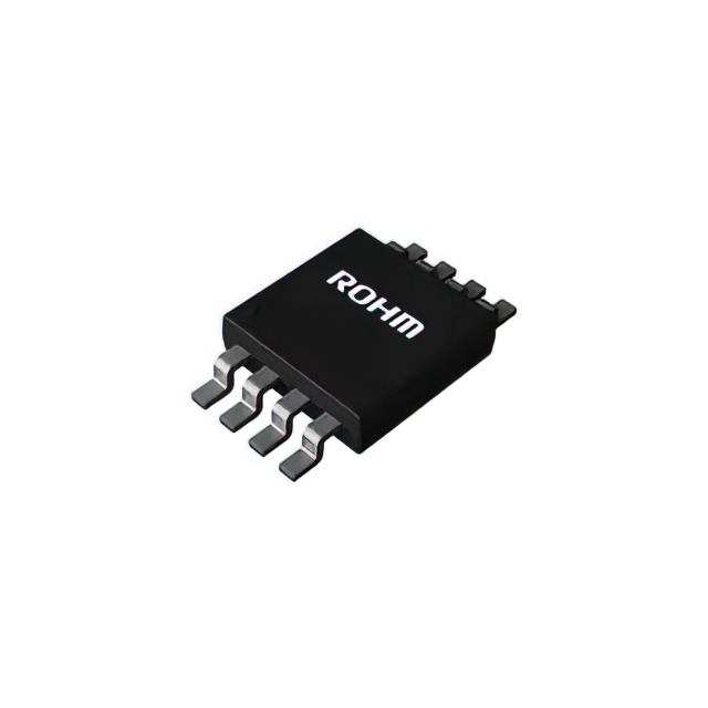
The BD14231FVJ-CE2 is an automotive-grade current sense amplifier from ROHM Semiconductor, designed for high-precision shunt-based current monitoring. It operates on a single power supply ranging from 2.7 V to 18 V and features a wide common-mode voltage range of -14 V to +80 V. The device provides a fixed typical gain of 50 V/V with a maximum gain accuracy of ±1.0%. Key electrical specifications include a quiescent current of 300 µA (typical), an input bias current of 1 µA (maximum), and an offset voltage of ±0.5 mV (maximum). It is housed in a TSSOP-B8J package and supports an operating temperature range from -40 °C to +125 °C.
Verify the specific suffix 'E2' corresponds to the embossed tape and reel packaging format required for automated assembly processes. Confirm that the 'C' designation aligns with the intended automotive application grade requirements. Ensure the ordering information matches the exact gain specification needed for the target circuit design before finalizing procurement.
Select this component when a fixed gain of 50 V/V is required for current sensing applications. Consider the TSSOP-B8J package dimensions if board space is constrained. Verify that the system's common-mode voltage does not exceed the specified limits relative to the power supply voltage. Evaluate thermal resistance characteristics against the expected ambient temperature conditions.
This part belongs to the BD1423x-C series of automotive current sense amplifiers. Other members in this family include variants with different gains such as 20 V/V and 100 V/V. The series shares similar architectural features including wide common-mode voltage handling and low offset characteristics, tailored for robust performance in demanding automotive environments.
Direct substitutes within the same series include BD14230FVJ-CE2 (20 V/V gain) and BD14232FVJ-CE2 (100 V/V gain). These parts share identical pinouts and packages but differ in internal gain settings. Cross-referencing with other manufacturers requires careful verification of gain accuracy, common-mode voltage ranges, and output swing characteristics.
REF1 and REF2 serve as reference voltage inputs. When connected to VDD and GND respectively, the output is referenced to half the supply voltage (VDD/2).
If current flows from VINM to VINP, the OUT pin voltage drops below the reference voltage level, allowing bidirectional current detection.
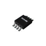 BD14231FVJ-CE2
The activity of extra discounts on wholesale prices is in full swing…
Please fill in your contact information and we will send you the latest wholesale price list.