 ChipApex | Global Electronic Components Supplier
SEARCH
Search Product
Search Post
— IC芯片 | 连接器 | 传感器 | 被动器件 —
Search productSearch post
— IC芯片 | 连接器 | 传感器 | 被动器件 —
Consult the customer manager about the wholesale price.
consultation hotline:86-132-6715-2157
email:[email protected]
Contact the product manager for consultation. One-stop consultation is available.
Do you want a lower wholesale price? Please send us your inquiry and we will reply immediately.
The BD9S300MUF-CE2 is a synchronous buck DC/DC converter from ROHM Semiconductor, designed for automotive applications. It integrates low on-resistance power MOSFETs to deliver a maximum output current of 3A. The device operates with an input voltage range of 2.7V to 5.5V and provides an adjustable output voltage between 800mV and 4.4V. Utilizing SLLM™ control technology, it ensures high efficiency in light-load conditions. The IC features a fixed switching frequency of 2.2MHz and supports external pulse synchronization. It is housed in a VQFN16-FV3030 package with wettable flanks and meets AEC-Q100 Grade 1 standards.
Verify the specific suffix CE2 confirms the wettable flank package variant required for automated assembly reliability. Confirm AEC-Q100 Grade 1 qualification aligns with target automotive environment specifications. Ensure the development kit BD9S300MUF-TSB-001 is available for initial circuit validation and thermal testing before mass production integration.
Select this component when a single-channel solution is required for 12V automotive bus architectures stepping down to lower logic voltages. The 3A capacity suits moderate load requirements without needing parallel configurations. The 2.2MHz frequency allows for smaller passive components compared to lower-frequency alternatives. Verify that the 2.7V minimum input voltage matches the lowest expected battery voltage under cranking or cold-start conditions.
This part belongs to the BD9S series of ROHM's Nano Pulse Control™ family, specifically engineered for automotive use. It shares the VQFN16-FV3030 footprint with other members like the BD9S402MUF-CE2, though output currents differ. The series emphasizes functional safety support and compact form factors suitable for space-constrained automotive PCB layouts.
The BD9S300MUF-C is the base part number without the specific manufacturing traceability suffix. Direct pin-compatible substitutes within the same ROHM family include the BD9S402MUF-CE2 for higher current needs, provided the input/output voltage ranges remain compatible with the application design constraints.
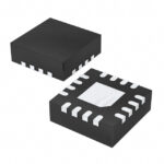 BD9S300MUF-CE2
The activity of extra discounts on wholesale prices is in full swing…
Please fill in your contact information and we will send you the latest wholesale price list.





