 ChipApex | Global Electronic Components Supplier
SEARCH
Search Product
Search Post
— IC芯片 | 连接器 | 传感器 | 被动器件 —
Search productSearch post
— IC芯片 | 连接器 | 传感器 | 被动器件 —
Consult the customer manager about the wholesale price.
consultation hotline:86-132-6715-2157
email:[email protected]
Contact the product manager for consultation. One-stop consultation is available.
Do you want a lower wholesale price? Please send us your inquiry and we will reply immediately.
The BR100/03,113 is a silicon bidirectional trigger device manufactured by NXP USA Inc., originally specified by Philips Semiconductors. Housed in the SOD27 glass envelope, it is designed for triac and thyristor trigger circuits. Key electrical parameters include a breakover voltage (V(BO)) ranging from 28 V to 36 V with a typical value of 32 V at 25 °C. The device supports a repetitive peak forward current (IFRM) of up to 2 A and delivers an output voltage (VO) of 7 V under a 20 Ω load. It features a breakover current of 50 μA maximum and a risetime of 1.5 μs. Thermal resistance from junction to ambient is typically 330 K/W, with a maximum operating junction temperature of 100 °C.
Verify the component origin as Philips Semiconductors or its successor entity NXP USA Inc. Confirm the package type matches the SOD27 outline dimensions provided in the specification. Ensure the ordering suffix corresponds to the specific reel or tape configuration required for assembly processes.
Select this device when a compact bidirectional trigger solution is required for low-power gate driving. Consider the 28 V to 36 V breakover voltage range to ensure compatibility with the target control circuit threshold. Verify that the 150 mW total power dissipation limit aligns with the thermal management capabilities of the host system design.
This component belongs to the family of silicon bidirectional trigger devices intended for phase control applications. It serves as a specialized interface between low-power control signals and high-power switching elements like triacs. The SOD27 package represents a small-outline transistor footprint adapted for this specific semiconductor function.
Cross-reference other silicon bidirectional trigger devices in the SOD27 package. Verify that substitute parts meet the 28 V to 36 V breakover voltage range and support the required 2 A repetitive peak forward current without exceeding the 100 °C junction temperature limit.
The breakover voltage symmetry is specified as a maximum difference of 3.5 V between positive and negative breakover voltages.
The output voltage is specified as 7 V when measured with a load resistance of 20 Ω in the test circuit defined in the datasheet.
The maximum storage temperature is 125 °C, while the minimum is -55 °C.
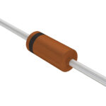 BR100/03,113
The activity of extra discounts on wholesale prices is in full swing…
Please fill in your contact information and we will send you the latest wholesale price list.





