 ChipApex | Global Electronic Components Supplier

SEARCH
Search Product
Search Post
— IC芯片 | 连接器 | 传感器 | 被动器件 —
Search productSearch post
— IC芯片 | 连接器 | 传感器 | 被动器件 —
Consult the customer manager about the wholesale price.
consultation hotline:86-132-6715-2157
email:[email protected]
Contact the product manager for consultation. One-stop consultation is available.
Do you want a lower wholesale price? Please send us your inquiry and we will reply immediately.
BSC016N04LSGATMA1 is listed in the Single FETs, MOSFETs range at ChipApex. The manufacturer field lists Infineon Technologies. Its product description is MOSFET N-CH 40V 31A/100A TDSON. Review the specifications below when checking this part for your BOM.
The BSC016N04LSGATMA1 is an OptiMOS™ 3 N-channel power MOSFET with a 40 V drain-source breakdown voltage. It features a maximum on-resistance of 1.6 mΩ at VGS=10 V and supports a continuous drain current of 100 A at TC=25 °C. The device utilizes a PG-TDSON-8 package, providing a thermal resistance from junction to case of 0.9 K/W. Key dynamic parameters include a total gate charge of 113 nC at VGS=10 V and a reverse recovery charge of 125 nC for the integrated body diode.
Verify that the ordering code matches the specific suffix G for the PG-TDSON-8 package configuration. Confirm compliance requirements including Pb-free plating, RoHS compliance, and halogen-free status per IEC61249-2-21. Ensure the procurement documentation references the correct datasheet revision Rev. 2.1 dated 2020-02-07 for accurate electrical parameter validation.
Select this component when a 40 V rating and low RDS(on) are required for high-current DC/DC conversion. The PG-TDSON-8 package offers a compact footprint with enhanced thermal performance suitable for vertical mounting on FR4 PCBs. Consider the 100 A continuous current capability at case temperature and the logic-level gate drive compatibility for efficient control circuit integration.
This part belongs to Infineon's OptiMOS™ 3 family of power transistors. It is manufactured using silicon technology and is housed in a surface-mount PG-TDSON-8 package. The device is designed as a single N-channel enhancement mode transistor intended for robust operation in demanding power electronics environments requiring high reliability and thermal stability.
Cross-reference with other OptiMOS 3 devices in the PG-TDSON-8 package offering similar 40 V ratings and comparable on-resistance values. Verify pinout compatibility and thermal resistance specifications before substituting to ensure adequate heat dissipation and electrical performance in the existing circuit layout.
The maximum pulsed drain current (ID,pulse) is 400 A at a case temperature of 25 °C.
The component is qualified according to JEDEC standards for target applications. However, use in life-support devices or automotive systems requires express written approval from Infineon Technologies.
The reverse recovery charge is typically 125 nC, measured at VR=20 V, IF=IS, and diF/dt=400 A/µs.
Explore related parts through FETs, MOSFETs, Transistors, Discrete Semiconductor Products, all product categories.
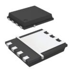 BSC016N04LSGATMA1

The activity of extra discounts on wholesale prices is in full swing…
Please fill in your contact information and we will send you the latest wholesale price list.





