 ChipApex | Global Electronic Components Supplier

SEARCH
Search Product
Search Post
— IC芯片 | 连接器 | 传感器 | 被动器件 —
Search productSearch post
— IC芯片 | 连接器 | 传感器 | 被动器件 —
Consult the customer manager about the wholesale price.
consultation hotline:86-132-6715-2157
email:[email protected]
Contact the product manager for consultation. One-stop consultation is available.
Do you want a lower wholesale price? Please send us your inquiry and we will reply immediately.
The BSS84PL6327HTSA1 is a dual N-channel MOSFET manufactured by Infineon Technologies, designed for low-voltage switching applications. It features a drain-source breakdown voltage (Vds) of 20 V and a continuous drain current (Id) of 880 mA. The device exhibits a maximum on-resistance (Rds(on)) of 270 mΩ at Vgs = 10 V and 373 mΩ at Vgs = 4.5 V. Key electrical parameters include a gate charge (Qg) of 260 pC, a threshold voltage (Vgs(th)) of 550 mV, and a power dissipation (Pd) of 500 mW. It operates within a temperature range of -55°C to +150°C and is housed in an SOT-363-6 package.
Verify the specific ordering suffix and packaging type against official Infineon documentation to ensure compatibility with automated assembly processes. Confirm that the component meets all required environmental and quality standards, such as AEC-Q100, for the intended application environment before finalizing procurement decisions.
Select this component when a dual N-channel MOSFET solution is required for low-voltage applications. Ensure the design accommodates the 20 V drain-source voltage limit and 880 mA current rating. Consider the SOT-363-6 package dimensions for PCB layout constraints and verify thermal management requirements based on the 500 mW power dissipation specification.
This part belongs to Infineon's portfolio of surface-mount MOSFETs, specifically tailored for automotive and industrial markets. It utilizes silicon technology and is designed to replace older discrete solutions by integrating two channels into one footprint, thereby reducing board space and simplifying assembly processes for manufacturers.
Publicly confirmed substitute part numbers are not available in the provided source material. Consult official Infineon cross-reference tools or datasheets for verified alternatives if this specific part number is unavailable.
The maximum drain-source voltage (Vds) is 20 V.
Yes, the component is qualified according to the AEC-Q100 standard.
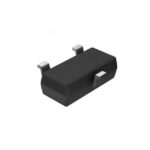 BSS84PL6327HTSA1

The activity of extra discounts on wholesale prices is in full swing…
Please fill in your contact information and we will send you the latest wholesale price list.





