 ChipApex | Global Electronic Components Supplier

SEARCH
Search Product
Search Post
— IC芯片 | 连接器 | 传感器 | 被动器件 —
Search productSearch post
— IC芯片 | 连接器 | 传感器 | 被动器件 —
Consult the customer manager about the wholesale price.
consultation hotline:86-132-6715-2157
email:[email protected]
Contact the product manager for consultation. One-stop consultation is available.
Do you want a lower wholesale price? Please send us your inquiry and we will reply immediately.
BY25D16ASTIG(T) is listed in the Memory IC range at ChipApex. The manufacturer field lists BYTe Semiconductor. Its product description is IC FLASH 16MBIT SPI/DUAL 8SOP. Review the specifications below when checking this part for your BOM.
The BY25D16ASTIG(T) is a 16M-bit SPI NOR Flash memory supporting Standard and Dual SPI interfaces. It operates on a single 2.7V to 3.6V supply. Read speeds include 55MHz for Normal Read, 108MHz for Fast Read, and 108MHz for Dual Output Fast Read. The device features a flexible architecture with 4KB sectors and 32/64KB blocks. Program/Erase times are 0.7ms typical for page programming, 100ms for sector erase, and 15s for chip erase. Active current is 20mA maximum, dropping to 5uA in power-down mode.
Verify the suffix 'T' indicates tube packaging when ordering. Confirm the temperature grade matches the application requirements, as industrial ranges vary. Ensure the voltage supply remains within the specified 2.7V to 3.6V range during operation. Check for RoHS compliance status if required by local regulations.
Select this component for designs requiring dual SPI interface support or specific block protection features. Consider the package options available, such as SOP or USON, based on board space constraints. Verify that the clock frequency requirements align with the supported read modes. Ensure the operating temperature range meets the environmental conditions of the target application.
This part belongs to the BYTe Semiconductor BY25D16AS family of 16M-bit SPI NOR Flash memories. It shares architectural similarities with other models in the series but differs in interface support and package options. The device is designed for high-reliability applications requiring robust write protection and fast read speeds.
Public confirmed substitute part numbers: None listed in source material.
Dual SPI uses bidirectional I/O pins (IO0 and IO1) to transfer data two bits per clock cycle, doubling the data rate compared to Standard SPI which uses separate input and output pins.
The Deep Power-Down instruction reduces standby current consumption significantly, making it suitable for battery-powered applications where minimizing power usage is critical.
Yes, by setting the Block Protect bits (BP2, BP1, BP0) to 111, all memory sectors can be protected against Page Program, Sector Erase, and Block Erase instructions.
Explore related parts through Memory, Integrated Circuits (ICs), all product categories, ChipApex homepage.
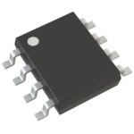 BY25D16ASTIG(T)

The activity of extra discounts on wholesale prices is in full swing…
Please fill in your contact information and we will send you the latest wholesale price list.







