 ChipApex | Global Electronic Components Supplier

SEARCH
Search Product
Search Post
— IC芯片 | 连接器 | 传感器 | 被动器件 —
Search productSearch post
— IC芯片 | 连接器 | 传感器 | 被动器件 —
Consult the customer manager about the wholesale price.
consultation hotline:86-132-6715-2157
email:[email protected]
Contact the product manager for consultation. One-stop consultation is available.
Do you want a lower wholesale price? Please send us your inquiry and we will reply immediately.
BY25D20ASTIG(R) is listed in the Memory IC range at ChipApex. The manufacturer field lists BYTe Semiconductor. Its product description is IC FLASH 2MBIT SPI/DUAL 8SOP. Review the specifications below when checking this part for your BOM.
The BY25D20ASTIG(R) is a 2M-bit SPI NOR Flash memory by BYTe Semiconductor. It supports Standard and Dual SPI interfaces with clock rates up to 55MHz for normal read and 108MHz for fast/dual read. Operating voltage ranges from 2.7V to 3.6V. Key performance metrics include a typical page program time of 0.7ms, sector erase time of 100ms, and block erase times of 0.3s or 0.5s. The device features a flexible architecture with 4KB sectors and 32/64KB blocks, low power consumption (20mA active, 5uA power down), and industrial temperature range support (-40°C to +85°C).
Verify the specific package variant (SOP-8, TSSOP-8, or USON-8) required for your design, as the base model number covers multiple packages. Confirm the suffix 'TIG(R)' corresponds to the exact tape-and-reel packaging and RoHS compliance status needed for your manufacturing process. Cross-reference the manufacturer ID (68h) and device ID (11h or 4012h depending on instruction) during component qualification to ensure authenticity and correct part identification.
Select this component if your application requires Dual SPI interface support for higher throughput without Quad I/O complexity. Ensure the system voltage stays within the 2.7V to 3.6V range. Consider the 0.7ms typical page program time for write-heavy workloads. Verify that the available packages (SOP-8, TSSOP-8, USON-8) fit your PCB layout constraints. Check if the industrial temperature range (-40°C to +85°C) is necessary for your operating environment.
The BY25D20AS series belongs to BYTe Semiconductor's 2M-bit SPI NOR Flash family. It is designed as a cost-effective solution for applications needing moderate density with dual-speed read capabilities. The series shares architectural similarities with other BY25DxxAS models but differs in density and specific package options. It competes in the general-purpose NOR Flash market for consumer and industrial electronics.
Check for direct equivalents from other manufacturers supporting Dual SPI and similar voltage ranges. Verify pin compatibility and command set adherence if substituting with different brands. Ensure the replacement supports the required 108MHz fast read speed and has comparable erase/program times.
The maximum clock frequency for Dual Output Fast Read is 108MHz.
Driving the WP pin low enables hardware protection for the Block Protect (BP2-BP0) and Status Register Protect (SRP) bits, making them read-only.
The typical page program time is 0.7ms.
Explore related parts through Memory, Integrated Circuits (ICs), all product categories, ChipApex homepage.
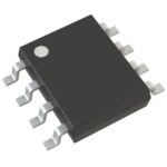 BY25D20ASTIG(R)

The activity of extra discounts on wholesale prices is in full swing…
Please fill in your contact information and we will send you the latest wholesale price list.





