 ChipApex | Global Electronic Components Supplier

SEARCH
Search Product
Search Post
— IC芯片 | 连接器 | 传感器 | 被动器件 —
Search productSearch post
— IC芯片 | 连接器 | 传感器 | 被动器件 —
Consult the customer manager about the wholesale price.
consultation hotline:86-132-6715-2157
email:[email protected]
Contact the product manager for consultation. One-stop consultation is available.
Do you want a lower wholesale price? Please send us your inquiry and we will reply immediately.
BY25Q80AWXIG(R) is listed in the Memory IC range at ChipApex. The manufacturer field lists BYTe Semiconductor. Its product description is IC FLASH 8MBIT SPI/QUAD 8USON. Review the specifications below when checking this part for your BOM.
The BY25Q80AW is an 8M-bit SPI NOR Flash memory designed for code shadowing and data storage. It supports Standard, Dual, and Quad SPI interfaces with clock rates up to 100MHz. The device operates on a single supply voltage ranging from 1.65V to 3.6V. Key specifications include a typical active current of 3mA and power-down current of 0.6uA. It features flexible architecture with 4KB sectors and 32/64KB blocks, supporting page programming up to 256 bytes. Endurance is rated at 10k cycles with 20-year data retention.
Verify the specific package variant (SOP8, TSSOP8, USON8) required for your design, as the datasheet lists multiple options. Confirm temperature grade availability (Commercial or Industrial). Check for end-of-life status or recommended new designs notices directly from BYTe Semiconductor before finalizing procurement plans.
Select this component when an 8M-bit capacity is needed with support for high-speed Quad SPI operations. Ensure the system voltage falls within the 1.65V to 3.6V range. Consider the available package types such as SOP8 or USON8 based on board space constraints. Verify that the required operating temperature range matches the Commercial or Industrial grades specified.
The BY25Q80AW belongs to the BY25Q series of SPI NOR Flash memories manufactured by BYTe Semiconductor. This series is engineered for high-volume consumer applications requiring reliable non-volatile storage. The device integrates JEDEC standard identification and unique serial numbers for traceability and system management.
Public confirmed substitute part numbers are not provided in the source material. Consult BYTe Semiconductor for direct equivalents or cross-reference compatible 8M-bit SPI NOR Flash devices with similar voltage and interface specifications.
The maximum clock rate for Fast Read operations is 100MHz.
When the QE bit is set to 1, the /WP and /HOLD pins function as IO2 and IO3 respectively for Quad SPI input and output.
The default page size is 256 bytes, but it can be configured to 512 bytes by setting the Dual Page (DP) bit in Status Register 3.
Explore related parts through Memory, Integrated Circuits (ICs), all product categories, ChipApex homepage.
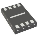 BY25Q80AWXIG(R)

The activity of extra discounts on wholesale prices is in full swing…
Please fill in your contact information and we will send you the latest wholesale price list.





