 ChipApex | Global Electronic Components Supplier

SEARCH
Search Product
Search Post
— IC芯片 | 连接器 | 传感器 | 被动器件 —
Search productSearch post
— IC芯片 | 连接器 | 传感器 | 被动器件 —
Consult the customer manager about the wholesale price.
consultation hotline:86-132-6715-2157
email:[email protected]
Contact the product manager for consultation. One-stop consultation is available.
Do you want a lower wholesale price? Please send us your inquiry and we will reply immediately.
BY25QM512FSZIG(Y) is listed in the Memory IC range at ChipApex. The manufacturer field lists BYTe Semiconductor. Its product description is IC FLSH 512MBIT SPI/QUAD 24TFBGA. Review the specifications below when checking this part for your BOM.
The BY25QM512FS is a 512M-bit Serial MCP Flash memory composed of two stacked 256M-bit BY25Q256FS dies within an 8-pin package. It supports Standard, Dual, Quad SPI, and QPI interfaces with DTR read capabilities reaching 400 Mbits/s. The device operates on a single 2.7V to 3.6V supply and features concurrent operations across dies. Key performance metrics include a typical page program time of 0.6ms, sector erase time of 50ms, and block erase times of 0.15s or 0.25s. It offers 100k program-erase cycles and 20-year data retention.
Verify the specific package variant required, as the datasheet lists 8-pad WSON (6x8mm), 16-pin SOP (300mil), and TFBGA options. Confirm that the ordering suffix matches the desired physical footprint and temperature range specifications before finalizing procurement orders.
Select this component when high-density storage is needed within strict pin-count constraints. The dual-die architecture provides superior throughput compared to single-die equivalents due to concurrent operation capabilities. Ensure the host controller supports the necessary SPI modes, including DTR and QPI, to utilize the maximum data transfer speeds.
This part belongs to the BY25Q series of Serial NOR Flash memories manufactured by BYTe Semiconductor. It utilizes a stacking technology to combine two BY25Q256FS dies into a single package, offering increased capacity without increasing the external interface complexity or pin count.
BY25QM512FSWIG(Y)
Explore related parts through Memory, Integrated Circuits (ICs), all product categories, ChipApex homepage.
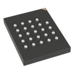 BY25QM512FSZIG(Y)

The activity of extra discounts on wholesale prices is in full swing…
Please fill in your contact information and we will send you the latest wholesale price list.





