 ChipApex | Global Electronic Components Supplier
SEARCH
Search Product
Search Post
— IC芯片 | 连接器 | 传感器 | 被动器件 —
Search productSearch post
— IC芯片 | 连接器 | 传感器 | 被动器件 —
Consult the customer manager about the wholesale price.
consultation hotline:86-132-6715-2157
email:[email protected]
Contact the product manager for consultation. One-stop consultation is available.
Do you want a lower wholesale price? Please send us your inquiry and we will reply immediately.
The Nexperia BZB84-C7V5-QR is a dual voltage regulator diode in the BZB84-Q series, housed in an SOT23 (TO-236AB) surface-mounted plastic package. It features a dual common anode configuration with two independent cathodes. The device provides a nominal Zener voltage of 7.5 V with approximately ±5% tolerance. Key electrical parameters include a total power dissipation of 300 mW, a non-repetitive peak reverse power dissipation of 40 W, and a maximum forward voltage of 0.9 V at 10 mA. It operates within a junction temperature range of -55 °C to +150 °C and is qualified according to AEC-Q101 standards for automotive applications.
Verify the specific ordering suffix against the manufacturer's current documentation to ensure correct packaging and tape-and-reel specifications. Confirm that the component meets all relevant RoHS directives and environmental compliance requirements for the intended deployment region before finalizing procurement orders.
Select this component when a dual-channel voltage reference or regulation solution is required in a space-constrained design. The dual common anode topology allows for efficient use of board area compared to discrete single diodes. Ensure the application current remains within the specified limits to maintain the stated voltage tolerance and thermal performance characteristics.
This part belongs to the Nexperia BZB84-Q series, which comprises 74 types of dual voltage regulator diodes. The series covers nominal working voltages from 2.4 V to 75 V in the E24 range. The 'Q' suffix indicates AEC-Q101 qualification, distinguishing it from standard commercial variants while maintaining the same physical SOT23 footprint and pinout configuration.
Direct replacements within the same family include BZB84-B7V5-Q for tighter tolerance requirements. Other series members like BZB84-C8V2-Q or BZB84-C6V8-Q may be used if different voltage levels are acceptable, provided the dual common anode configuration and SOT23 package remain compatible with the existing PCB layout.
Pin 1 is Cathode 1 (K1), Pin 2 is Cathode 2 (K2), and Pin 3 is the Common Anode (CA).
Yes, the device is qualified according to the AEC-Q101 stress test qualification for discrete semiconductors and is recommended for use in automotive applications.
The total power dissipation (Ptot) per device is limited to 300 mW at an ambient temperature of 25 °C.
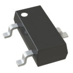 BZB84-C7V5-QR
The activity of extra discounts on wholesale prices is in full swing…
Please fill in your contact information and we will send you the latest wholesale price list.




