ChipApex | Global Electronic Components Supplier
SEARCH
Search Product
Search Post
— IC芯片 | 连接器 | 传感器 | 被动器件 —
Search productSearch post
— IC芯片 | 连接器 | 传感器 | 被动器件 —
Consult the customer manager about the wholesale price.
consultation hotline:86-132-6715-2157
email:[email protected]
Contact the product manager for consultation. One-stop consultation is available.
Do you want a lower wholesale price? Please send us your inquiry and we will reply immediately.
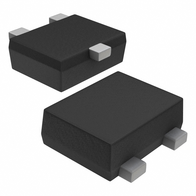
The Nexperia BZB984-C7V5,115 is a voltage regulator double diode housed in an ultra-small SOT663 plastic surface-mounted device package. It provides dual Zener regulation with a nominal working voltage of 7.5 V and a tolerance of approximately 5%. The component supports a total power dissipation of up to 425 mW when both diodes are loaded at temperatures ≤ 25 °C, or 265 mW for single-diode operation. Key electrical characteristics include a maximum forward voltage of 0.9 V at 10 mA, a non-repetitive peak reverse current of 150 A (at 100 µs pulse), and a junction temperature limit of 150 °C.
Verify the specific ordering suffix matches the required tape-and-reel quantity configuration before finalizing procurement orders. Confirm that the application environment remains within the specified non-automotive qualification limits, as this product lacks automotive reliability testing. Ensure thermal management strategies account for the stated thermal resistance values under actual PCB mounting conditions.
Select this component when dual independent voltage references or clamping paths are required in a minimal footprint. The SOT663 package is suitable for high-density circuit boards where standard discrete packages exceed available space. Consider the 5% tolerance band for applications requiring moderate precision without the cost of tighter grading options.
This part belongs to the BZB984 series of low-power voltage regulator double diodes manufactured by Nexperia. The series offers various nominal voltages ranging from 2.4 V to 15 V, all sharing the same SOT663 package outline and pinning configuration. It serves as a compact alternative to using two separate single Zener diodes in voltage reference or protection circuits.
Direct functional replacements must match the SOT663 package, 7.5 V nominal voltage, and dual-diode configuration. Verify that any substitute component meets the 425 mW total power dissipation requirement and maintains compatible thermal resistance characteristics for the intended PCB layout.
 BZB984-C7V5,115
The activity of extra discounts on wholesale prices is in full swing…
Please fill in your contact information and we will send you the latest wholesale price list.