 ChipApex | Global Electronic Components Supplier
SEARCH
Search Product
Search Post
— IC芯片 | 连接器 | 传感器 | 被动器件 —
Search productSearch post
— IC芯片 | 连接器 | 传感器 | 被动器件 —
Consult the customer manager about the wholesale price.
consultation hotline:86-132-6715-2157
email:[email protected]
Contact the product manager for consultation. One-stop consultation is available.
Do you want a lower wholesale price? Please send us your inquiry and we will reply immediately.
The C8051F230 is a mixed-signal System on a Chip MCU featuring an 8051-compatible core with 8 kB of in-system programmable Flash memory and 256 bytes of internal data RAM. It operates at up to 25 MIPS with a 25 MHz clock, supporting a supply voltage range of 2.7 V to 3.6 V. The device includes hardware UART and SPI interfaces, three 16-bit counter/timers, and a dedicated watchdog timer. It provides 32 general-purpose I/O pins that are 5 V tolerant and supports full-speed non-intrusive JTAG debugging.
Verify the specific package variant, as the C8051F2xx family offers both 48-pin TQFP and 32-pin LQFP options. Confirm the operating temperature range requirements against the standard -40 °C to +85 °C specification. Ensure development tools support the CIP-51 core architecture for proper programming and debugging integration.
Select this model when ADC functionality is not required, distinguishing it from other members of the C8051F2xx family. It is suitable for applications prioritizing digital I/O count and serial peripherals over analog signal acquisition. Consider the 5 V tolerant I/O capability if interfacing with legacy logic levels directly.
The C8051F230 belongs to the C8051F2xx family of fully integrated mixed-signal System on a Chip MCUs manufactured by Silicon Laboratories. This family shares a common high-speed 8051 core and ISP Flash technology, differentiating models primarily through the inclusion or exclusion of analog peripherals like multi-channel ADCs and comparators.
No public confirmed substitute part numbers are available in the provided documentation.
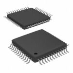 C8051F230
The activity of extra discounts on wholesale prices is in full swing…
Please fill in your contact information and we will send you the latest wholesale price list.







