 ChipApex | Global Electronic Components Supplier
SEARCH
Search Product
Search Post
— IC芯片 | 连接器 | 传感器 | 被动器件 —
Search productSearch post
— IC芯片 | 连接器 | 传感器 | 被动器件 —
Consult the customer manager about the wholesale price.
consultation hotline:86-132-6715-2157
email:[email protected]
Contact the product manager for consultation. One-stop consultation is available.
Do you want a lower wholesale price? Please send us your inquiry and we will reply immediately.
The C8051F352-GQR is an 8-bit microcontroller from the Silicon Labs C8051F35x family, featuring a high-speed 50 MIPS CIP-51 core. It integrates 8 kB of in-system programmable Flash memory and 768 bytes of on-chip RAM. The device includes a 16-bit sigma-delta ADC subsystem with up to eight input channels and a programmable gain stage, alongside two separate 8-bit current-output DACs. Operating within a supply voltage range of 2.7V to 3.6V, it supports digital interfaces including SMBus, SPI, and UART/USART. The component is housed in a 32-LQFP package.
Verify component authenticity through authorized distribution channels due to end-of-life status. Confirm package integrity upon receipt as the device utilizes surface-mount technology. Ensure compatibility with existing firmware architectures given the specific peripheral configuration of the C8051F35x series. Review official documentation for any recent design rule changes affecting thermal management or signal routing.
Select this component for designs prioritizing integrated analog peripherals over high pin counts. The 32-pin LQFP package limits available I/O compared to larger packages in the same family. Evaluate power consumption requirements against the specified operating currents at varying clock frequencies. Consider the availability of development kits for initial prototyping and debugging support.
This part belongs to the C8051F35x series of mixed-signal microcontrollers designed for cost-sensitive applications. The series shares a common architectural foundation but varies in memory size and peripheral sets. The C8051F352 specifically targets applications needing moderate Flash capacity with robust analog conversion capabilities. It represents a mature product line within Silicon Labs' portfolio of fully integrated system-on-chip solutions.
EFM8BB31F64I-D-QFN32R is a confirmed public substitute option. Verify pinout compatibility and software migration efforts when transitioning to alternative members of the C8051F35x family or newer generations.
The ADC subsystem supports programmable conversion rates up to 1 ksps.
Yes, the Flash memory can be reprogrammed even in-circuit, allowing for field upgrades of the firmware.
The device supports an internal oscillator with 24.5 MHz accuracy, external crystals, RC circuits, capacitors, or external clock signals.
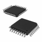 C8051F352-GQR
The activity of extra discounts on wholesale prices is in full swing…
Please fill in your contact information and we will send you the latest wholesale price list.







