ChipApex | Global Electronic Components Supplier

SEARCH
Search Product
Search Post
— IC芯片 | 连接器 | 传感器 | 被动器件 —
Search productSearch post
— IC芯片 | 连接器 | 传感器 | 被动器件 —
Consult the customer manager about the wholesale price.
consultation hotline:86-132-6715-2157
email:[email protected]
Contact the product manager for consultation. One-stop consultation is available.
Do you want a lower wholesale price? Please send us your inquiry and we will reply immediately.
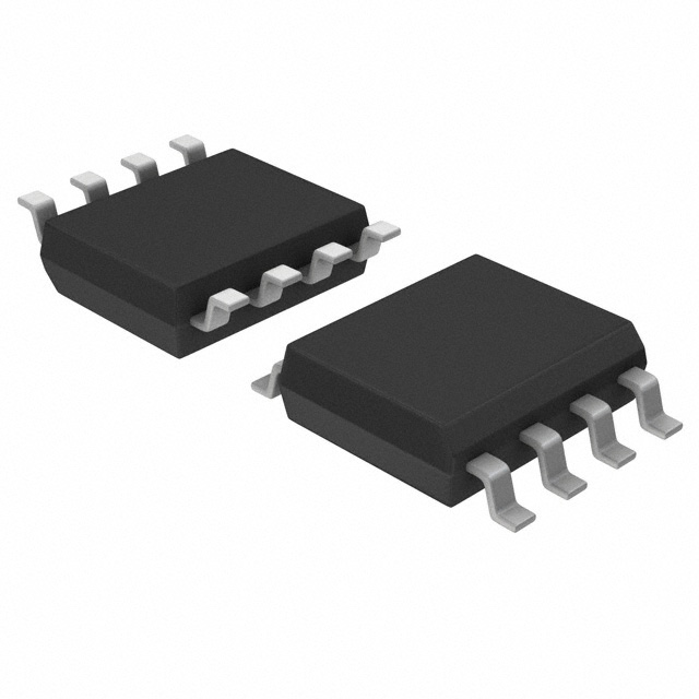
CAT25512XI-T2 is listed in the Memory IC range at ChipApex. The manufacturer field lists onsemi. Its product description is IC EEPROM 512KBIT SPI 8SOIC. Review the specifications below when checking this part for your BOM.
The CAT25512XI-T2 is a 512-Kb (64K x 8) serial EEPROM from onsemi, packaged in an SOIC-8 (X suffix). It supports SPI protocol modes (0,0) and (1,1) with a maximum clock frequency of 20 MHz. The device operates within a supply voltage range of 1.8 V to 5.5 V and features a 128-byte page write buffer. It includes hardware and software write protection, block protection for quarter, half, or full array segments, and an additional identification page. The component offers 1,000,000 program/erase cycles and 100-year data retention.
Verify the specific package suffix 'X' corresponds to the SOIC-8 EIAJ case 751BE when sourcing. Confirm that the operating temperature range aligns with industrial specifications (-40°C to +85°C). Ensure the design accounts for the required power-up delay before initiating read or write operations. Check status register bits for correct write enable and block protection settings during integration.
Select this component for designs requiring a 512-Kb capacity with SPI compatibility. The X suffix indicates the SOIC-8 package variant suitable for surface mount assembly. Consider the 1.8 V to 5.5 V supply range for flexibility in system voltage architectures. Evaluate the need for the dedicated identification page if firmware versioning or unique device identifiers are required.
This part belongs to the CAT25512 family of serial EEPROMs manufactured by onsemi. The family provides various packaging options including SOIC, TSSOP, and UDFN. The XI-T2 designation specifically identifies the industrial temperature grade, SOIC-8 package, and tape-and-reel shipping format. It serves as a drop-in replacement for other 512-Kb SPI EEPROMs with compatible pinouts and command sets.
Compatible substitutes include CAT25512VI-GT3 and CAT25512YE-GT3, which share identical electrical characteristics but differ in package type (SOIC JEDEC and TSSOP respectively). Verify pinout compatibility and ensure the alternative package meets mechanical constraints of the target PCB layout.
The HOLD pin allows pausing serial communication without retransmitting the sequence. To pause, HOLD must be taken low while SCK is low. During hold, the SO output is tri-stated and SI transitions are ignored. Communication resumes when HOLD is taken high while SCK is low.
The Identification Page is an additional 128-byte memory area accessible via the IPL bit in the Status Register. It can be used for storing user data or device information and can be permanently write-protected using the LIP bit.
Write protection is managed through the WPEN, WP, BP0, and BP1 bits in the Status Register. Hardware protection is enabled when WPEN is set and the WP pin is low. Block protection allows protecting one-quarter, one-half, or the entire array against writes.
Explore related parts through Memory, Integrated Circuits (ICs), all product categories, ChipApex homepage.
 CAT25512XI-T2

The activity of extra discounts on wholesale prices is in full swing…
Please fill in your contact information and we will send you the latest wholesale price list.