 ChipApex | Global Electronic Components Supplier
SEARCH
Search Product
Search Post
— IC芯片 | 连接器 | 传感器 | 被动器件 —
Search productSearch post
— IC芯片 | 连接器 | 传感器 | 被动器件 —
Consult the customer manager about the wholesale price.
consultation hotline:86-132-6715-2157
email:[email protected]
Contact the product manager for consultation. One-stop consultation is available.
Do you want a lower wholesale price? Please send us your inquiry and we will reply immediately.
The CBTL02GP023 is a one-port, high-performance 5 Gbps rail-to-rail low insertion loss switch chip designed for USB 3.0 signal interfacing with high-voltage off-isolation. It supports differential channels with a typical bandwidth of 7 GHz and an ON-state resistance of 11 Ω. The device operates within a VDD supply range of 2.7 V to 3.5 V, consuming a maximum active current of 500 μA. It features low insertion loss of -1.5 dB at 2.5 GHz and offers ESD protection exceeding 2000 V HBM. Packaged in a DHX2QFN14 (1.5 mm x 2.1 mm x 0.32 mm) format, it functions across an ambient temperature range of -20 °C to +85 °C.
Verify the specific ordering suffix HOZ corresponds to the REEL 13" Q1/T1 packing method as documented in the NXP datasheet. Confirm that the component meets the required operating temperature range of -20 °C to +85 °C for your specific environmental conditions. Ensure design compatibility with the DHX2QFN14 package dimensions and soldering profiles specified in the official documentation.
Select this component when interfacing 5 Gbps USB 3.0 data lines with higher voltage domains requiring significant off-isolation. The rail-to-rail input characteristic allows compatibility with various signal swings, including USB 2.0 and UART. Consider the small form factor and low active current consumption if space and power efficiency are critical constraints in the target application design.
The CBTL02GP023 belongs to NXP's CBTL series of high-speed analog switches. It is specifically engineered for portable electronics and connectivity interfaces where signal integrity at 5 Gbps is paramount. The device utilizes patent-pending analog pass-gate technology to achieve its performance metrics while maintaining a compact footprint suitable for modern miniaturized hardware designs.
No direct public substitute part numbers are listed in the provided datasheet. Engineers should consult NXP technical support or review the broader CBTL family specifications for potential alternatives that match the required pinout, electrical characteristics, and package dimensions.
When ENH is LOW, the switches enter a high-impedance sleep mode with a maximum current consumption of 12 μA. When HIGH, the device enables the switches with a maximum current consumption of 500 μA.
The common mode input voltage (VIC) for all switch ports ranges from 0 V to VDD, allowing for rail-to-rail operation.
The typical intra-pair skew for the differential channels is 6 ps.
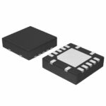 CBTL02GP023HOZ
The activity of extra discounts on wholesale prices is in full swing…
Please fill in your contact information and we will send you the latest wholesale price list.





