 ChipApex | Global Electronic Components Supplier
SEARCH
Search Product
Search Post
— IC芯片 | 连接器 | 传感器 | 被动器件 —
Search productSearch post
— IC芯片 | 连接器 | 传感器 | 被动器件 —
Consult the customer manager about the wholesale price.
consultation hotline:86-132-6715-2157
email:[email protected]
Contact the product manager for consultation. One-stop consultation is available.
Do you want a lower wholesale price? Please send us your inquiry and we will reply immediately.
The CBTU02044 is a high-speed differential 1-to-2 switch optimized for PCIe Gen4 interfaces in server and client applications. It supports two differential channels with a 3 dB bandwidth of 17 GHz, low insertion loss (0.56 dB at 100 MHz), and off-state isolation of -70 dB at 100 MHz. The device operates on a VDD supply voltage range of 1.62 V to 3.63 V, consuming 200 μA in active mode and 3 μA in power-saving mode. It features rail-to-rail input support up to 2.4 V, back current protection, and an ESD rating of 2000 V HBM. Packaged in a HUQFN16 footprint measuring 1.6 mm x 2.4 mm x 0.5 mm, it functions as both a 1-to-2 switch and a 2-to-1 MUX.
Verify the specific ordering suffix HEJ corresponds to the required reel packing method and standard marking configuration. Confirm that the HUQFN16 package dimensions align with the PCB footprint design guidelines provided in the datasheet. Ensure environmental operating conditions meet the specified temperature range of -40 °C to +85 °C for the target application environment.
Select this component when designing high-speed differential signal paths requiring minimal insertion loss and strict crosstalk control. The integrated shutdown pin allows for efficient power management in battery-operated or energy-sensitive systems. Verify compatibility with the host controller's GPIO levels for SEL and XSD control signals before finalizing the schematic design.
This part belongs to NXP's portfolio of high-speed analog switches designed for modern computing infrastructure. It addresses the increasing bandwidth demands of next-generation interconnects like PCIe Gen4. The device integrates advanced analog pass-gate technology to maintain signal fidelity across wide frequency ranges while occupying minimal board real estate.
No direct public substitute part numbers are documented in the official datasheet. Designers should evaluate other NXP high-speed switches based on matching pinout compatibility, electrical specifications, and package dimensions if replacement is necessary.
The device enters a high-impedance state with minimized supply current consumption when the XSD pin is driven HIGH. When XSD is LOW, the device operates normally.
All channels support rail-to-rail input voltages up to 2.4 V, allowing compatibility with various logic levels without external level shifting.
Yes, it can operate as a 2-to-1 MUX by selecting Port A as the output from either Port B or Port C, controlled via the SEL pin.
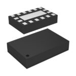 CBTU02044HEJ
The activity of extra discounts on wholesale prices is in full swing…
Please fill in your contact information and we will send you the latest wholesale price list.





