 ChipApex | Global Electronic Components Supplier
SEARCH
Search Product
Search Post
— IC芯片 | 连接器 | 传感器 | 被动器件 —
Search productSearch post
— IC芯片 | 连接器 | 传感器 | 被动器件 —
Consult the customer manager about the wholesale price.
consultation hotline:86-132-6715-2157
email:[email protected]
Contact the product manager for consultation. One-stop consultation is available.
Do you want a lower wholesale price? Please send us your inquiry and we will reply immediately.
The CBTU04082BS,518 is an 8-to-4 differential channel multiplexer/demultiplexer switch designed for high-speed serial interfaces. It routes four differential signals to one of two locations with negligible attenuation and minimal skew. The device operates within a VDD range of 1.8 V ± 10 % (1.7 V to 1.9 V). Key electrical parameters include a maximum data rate of 5.0 Gbit/s, a -3 dB bandwidth of 4.1 GHz, and a propagation delay of 80 ps typical. Signal integrity is maintained through low intra-pair skew (10 ps max) and inter-pair skew (35 ps max). Crosstalk and off-state isolation are both specified at -23 dB at 3 GHz. The component features ESD tolerance of 6 kV HBM and 1 kV CDM, housed in an HVQFN42 package.
Verify the specific ordering suffix BS against the manufacturer's current documentation to confirm the exact package variant and tape-and-reel specifications. Confirm that the moisture sensitivity level and shelf life requirements align with your assembly timeline. Ensure that the procurement source provides valid traceability documentation consistent with NXP Semiconductors standards for this product line.
Select this component when designing systems requiring low-loss routing of multiple differential pairs to dual destinations. The single enable pin simplifies control logic compared to multi-enable alternatives. Verify that the system power supply strictly adheres to the 1.8 V ± 10 % specification to maintain optimal dynamic characteristics and prevent exceeding absolute maximum ratings during operation.
This part belongs to NXP's CBTL/CBTU series of high-speed analog switches. These components are engineered specifically for preserving signal integrity in high-frequency digital environments. The family offers various channel counts and form factors, allowing designers to scale connectivity solutions while maintaining consistent electrical performance profiles across different application densities.
The datasheet explicitly states fit, form, and function compatibility with the PI2PCIE2412. Designers may consider this alternative if sourcing constraints exist, provided that the substitute meets the same 1.8 V operating voltage and HVQFN42 package dimensions without requiring PCB layout modifications.
The device supports high-speed signal switching up to 5.0 Gbit/s.
When SEL is Low, signals route from Port A to Port B. When SEL is High, signals route from Port A to Port C.
The typical propagation delay from the left-side port to the right-side port, or vice versa, is 80 ps.
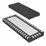 CBTU04082BS,518
The activity of extra discounts on wholesale prices is in full swing…
Please fill in your contact information and we will send you the latest wholesale price list.





