 ChipApex | Global Electronic Components Supplier

SEARCH
Search Product
Search Post
— IC芯片 | 连接器 | 传感器 | 被动器件 —
Search productSearch post
— IC芯片 | 连接器 | 传感器 | 被动器件 —
Consult the customer manager about the wholesale price.
consultation hotline:86-132-6715-2157
email:[email protected]
Contact the product manager for consultation. One-stop consultation is available.
Do you want a lower wholesale price? Please send us your inquiry and we will reply immediately.
CD4511BCN is listed in the Display Drivers range at ChipApex. The manufacturer field lists onsemi. Its product description is IC DRVR 7 SEGMENT 16DIP. Review the specifications below when checking this part for your BOM.
The onsemi CD4511BCN is a CMOS BCD-to-7-segment latch/decoder/driver designed for common-cathode LED displays. It operates within a supply voltage range of 3V to 15V and draws a typical supply current of 10 µA. The device is housed in a 16-PDIP package with a pin pitch of 0.300 inches (7.62mm). It supports an operating temperature range from -55°C to 125°C. This component provides direct drive capability for seven-segment indicators, integrating latching, decoding, and output driving functions into a single integrated circuit.
Verify component authenticity as this part number is obsolete. Confirm package integrity upon receipt. Check datasheet revisions for electrical parameter variations between original and successor manufacturers. Ensure compatibility with existing PCB footprints when transitioning to replacement sources.
Select this component for designs requiring hardware-based BCD translation to reduce processor load. Verify that the target display is common-cathode compatible. Ensure the system power supply remains within the specified 3V to 15V range. Consider thermal dissipation limits if operating at maximum ambient temperatures or utilizing multiple units simultaneously.
This device belongs to the standard CD4511 family of CMOS logic devices. It serves as a foundational building block for discrete digital display systems. The 'BCN' suffix typically denotes a specific plastic dual-in-line package variant manufactured by onsemi. It represents a legacy solution for simple numeric indication tasks before widespread adoption of multiplexed driver ICs.
Texas Instruments CD4511BE is a confirmed direct substitute. Verify pinout compatibility and electrical specifications against the original datasheet before implementation.
When the Blanking Input (BI) is high and the LT pin is low, all segment outputs are forced high, illuminating all segments to verify display functionality regardless of BCD input status.
When LE is low, the decoder responds to input changes. When LE transitions high, the current BCD input is latched, holding the display constant even if subsequent input signals fluctuate.
The internal logic includes a blanking mechanism that suppresses output for BCD inputs ranging from 1010 to 1111, preventing undefined character patterns on the display.
Explore related parts through Power Management (PMIC), Integrated Circuits (ICs), all product categories, ChipApex homepage.
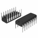 CD4511BCN

The activity of extra discounts on wholesale prices is in full swing…
Please fill in your contact information and we will send you the latest wholesale price list.





