 ChipApex | Global Electronic Components Supplier

SEARCH
Search Product
Search Post
— IC芯片 | 连接器 | 传感器 | 被动器件 —
Search productSearch post
— IC芯片 | 连接器 | 传感器 | 被动器件 —
Consult the customer manager about the wholesale price.
consultation hotline:86-132-6715-2157
email:[email protected]
Contact the product manager for consultation. One-stop consultation is available.
Do you want a lower wholesale price? Please send us your inquiry and we will reply immediately.
The CD74ACT74M is a dual D-type edge-triggered flip-flop from Texas Instruments' ACT logic series. It features independent data (D), clock (CLK), set (SET), and reset (RESET) inputs for each of its two circuits, providing complementary Q and /Q outputs. The device operates within a supply voltage range of 1.5 V to 5.5 V, with typical operation at 5 V. It utilizes a 14-pin SOIC package for surface-mount installation. Key electrical parameters include a maximum propagation delay of 125 ns at 5 V with a 50 pF load, and output drive capabilities of -24 mA high and 24 mA low. The component supports a wide operating temperature range from -55 °C to +125 °C.
Verify the specific suffix against the manufacturer's current documentation to confirm pinout compatibility and electrical characteristics. Ensure the selected variant matches the required package type and temperature rating for the target application environment. Cross-reference the ordering information with official datasheets to avoid discrepancies between legacy part numbers and current production versions.
Select this component when dual independent storage elements are required within a single package footprint. The ACT series offers speed-performance comparable to standard TTL while maintaining CMOS power efficiency. Consider the asynchronous control inputs for applications requiring immediate state overrides without clock synchronization. Evaluate the 1.5 V to 5.5 V operating range to ensure compatibility with the system's power supply architecture.
The CD74ACT74M belongs to the CD74ACT family of high-speed CMOS logic devices manufactured by Texas Instruments. This series is designed to provide performance levels similar to classic TTL logic but with the lower power consumption and wider voltage tolerance characteristic of CMOS technology. The ACT family is widely used in digital systems requiring reliable state retention and fast switching speeds across industrial and commercial temperature ranges.
CD74ACT74DR
The set and reset functions are asynchronous, meaning they override the clock and data inputs to immediately force the output to a defined state.
The maximum operating supply voltage is 5.5 V, although the device is typically operated at 5 V for optimal performance matching TTL standards.
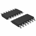 CD74ACT74M

The activity of extra discounts on wholesale prices is in full swing…
Please fill in your contact information and we will send you the latest wholesale price list.





