 ChipApex | Global Electronic Components Supplier

SEARCH
Search Product
Search Post
— IC芯片 | 连接器 | 传感器 | 被动器件 —
Search productSearch post
— IC芯片 | 连接器 | 传感器 | 被动器件 —
Consult the customer manager about the wholesale price.
consultation hotline:86-132-6715-2157
email:[email protected]
Contact the product manager for consultation. One-stop consultation is available.
Do you want a lower wholesale price? Please send us your inquiry and we will reply immediately.
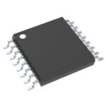
CD74HC4094PWT is listed in the Shift Registers range at ChipApex. The manufacturer field lists Texas Instruments. Its product description is IC 8STG BUS REG TRI-ST 16-TSSOP. Review the specifications below when checking this part for your BOM.
The CD74HC4094PWT is an 8-stage serial shift register with a storage latch and three-state parallel outputs, manufactured by Texas Instruments. It operates within a supply voltage range of 2V to 6V and supports an operating temperature range of -55°C to 125°C. The device features buffered inputs and two separate serial outputs (QS1 and QS2) for cascading. QS1 provides data on positive clock edges, while QS2 provides data on negative clock edges. The package is a 16-pin TSSOP.
Verify the complete part number including suffixes when ordering. The 'T' suffix denotes a small-quantity reel configuration. Confirm the specific package type and temperature range requirements against the datasheet specifications before procurement to ensure compatibility with the target application environment.
Select this component for designs requiring serial-to-parallel conversion with latched outputs. The HC variant supports 2V to 6V operation, suitable for various CMOS logic families. Consider the QS1 and QS2 outputs for flexible cascading options depending on clock signal characteristics and system timing requirements.
This device belongs to the Texas Instruments High-Speed CMOS Logic family. It is functionally compatible with other 74HC4094 variants in terms of logic operations but differs in packaging and reel quantity. The PWT designation specifically indicates the TSSOP package form factor with a small-quantity reel packing method.
CD74HC4094PW
QS1 outputs data on the positive clock edge, suitable for high-speed cascading. QS2 outputs data on the next negative clock edge, providing a means for cascading devices when the clock rise time is slow.
Data in each shift register stage is transferred to the storage register when the Strobe input is high. This allows the parallel outputs to update simultaneously without intermediate states.
Explore related parts through Logic, Integrated Circuits (ICs), all product categories, ChipApex homepage.
 CD74HC4094PWT

The activity of extra discounts on wholesale prices is in full swing…
Please fill in your contact information and we will send you the latest wholesale price list.





