 ChipApex | Global Electronic Components Supplier

SEARCH
Search Product
Search Post
— IC芯片 | 连接器 | 传感器 | 被动器件 —
Search productSearch post
— IC芯片 | 连接器 | 传感器 | 被动器件 —
Consult the customer manager about the wholesale price.
consultation hotline:86-132-6715-2157
email:[email protected]
Contact the product manager for consultation. One-stop consultation is available.
Do you want a lower wholesale price? Please send us your inquiry and we will reply immediately.
The CDC2351DBR is a single-circuit fanout buffer manufactured by Texas Instruments, designed for clock distribution applications. It accepts a single-ended LVTTL input and provides ten single-ended LVTTL outputs with tri-state capability. The device operates within a supply voltage range of 3V to 3.6V and supports maximum frequencies up to 100 MHz. It is housed in a 24-SSOP package (5.30mm width) and is rated for an operating temperature range of 0°C to 70°C.
Verify the specific package variant against project requirements, as the manufacturer offers both Tape & Reel (TR) and Bulk packaging options for this component. Confirm that the commercial temperature range (0°C to 70°C) aligns with the operational environment constraints before finalizing procurement decisions.
Select this component when a single-ended LVTTL interface is required for driving multiple loads. Ensure the design accommodates the 3V to 3.6V supply voltage range. Consider the 24-SSOP footprint dimensions (5.30mm width) during PCB layout planning to ensure adequate clearance and routing space.
This part belongs to the clock buffer category within Texas Instruments' portfolio. It serves as a distribution element for converting one input signal into ten buffered output signals, facilitating signal integrity maintenance across digital logic circuits without requiring differential signaling interfaces.
Publicly confirmed substitute part numbers are not available in the provided source material.
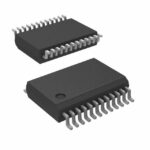 CDC2351DBR

The activity of extra discounts on wholesale prices is in full swing…
Please fill in your contact information and we will send you the latest wholesale price list.




