 ChipApex | Global Electronic Components Supplier

SEARCH
Search Product
Search Post
— IC芯片 | 连接器 | 传感器 | 被动器件 —
Search productSearch post
— IC芯片 | 连接器 | 传感器 | 被动器件 —
Consult the customer manager about the wholesale price.
consultation hotline:86-132-6715-2157
email:[email protected]
Contact the product manager for consultation. One-stop consultation is available.
Do you want a lower wholesale price? Please send us your inquiry and we will reply immediately.
The CDC2351QDB is an automotive-grade fanout buffer manufactured by Texas Instruments, designed for clock distribution applications. It provides a single circuit with a 1:10 input-to-output ratio, supporting maximum frequencies up to 100 MHz. The device accepts LVTTL inputs and generates LVTTL outputs, operating within a supply voltage range of 3 V to 3.6 V. Qualified under AEC-Q100 standards, it functions reliably across an extended temperature range from -40°C to +125°C. Packaged in a 24-SSOP surface-mount case, this component ensures signal integrity in demanding automotive electronic environments.
Verify the specific ordering suffix 'QDB' against the manufacturer's official documentation to confirm package type and tape/reel specifications. Ensure the procurement channel provides valid AEC-Q100 certification records. Confirm that the delivered components match the 24-SSOP physical dimensions and electrical parameters specified in the datasheet before integration into production lines.
Select the CDC2351QDB when an automotive-rated clock buffer with a 1:10 split ratio is required. It is suitable for designs needing LVTTL signaling at frequencies up to 100 MHz. Consider this part if the application demands operation in high-temperature environments up to 125°C. Verify that the 3V to 3.6V supply range aligns with the system power architecture.
This component belongs to the CDC235x series of clock buffers and drivers from Texas Instruments. The 'Q' prefix typically denotes automotive grade qualification, while 'DB' indicates the 24-SSOP package. It serves as a specialized variant within the broader CDC family, tailored specifically for automotive reliability standards rather than general consumer or industrial use.
Check for direct cross-references within the CDC235x family. Verify pinout compatibility and electrical characteristics such as propagation delay and output drive strength before substituting with other 1:10 fanout buffers.
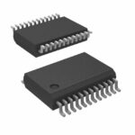 CDC2351QDB

The activity of extra discounts on wholesale prices is in full swing…
Please fill in your contact information and we will send you the latest wholesale price list.






