 ChipApex | Global Electronic Components Supplier

SEARCH
Search Product
Search Post
— IC芯片 | 连接器 | 传感器 | 被动器件 —
Search productSearch post
— IC芯片 | 连接器 | 传感器 | 被动器件 —
Consult the customer manager about the wholesale price.
consultation hotline:86-132-6715-2157
email:[email protected]
Contact the product manager for consultation. One-stop consultation is available.
Do you want a lower wholesale price? Please send us your inquiry and we will reply immediately.
The CDC2351QDBG4 is an automotive-grade fanout buffer manufactured by Texas Instruments, designed for clock distribution applications. It features a 1:10 input-to-output ratio, accepting LVTTL inputs and providing ten LVTTL outputs. The device supports a maximum operating frequency of 100 MHz and functions within a supply voltage range of 3V to 3.6V. Qualified under AEC-Q100 standards, it ensures reliability in demanding environments with an extended operating temperature range from -40°C to +125°C. The component is housed in a 24-SSOP surface-mount package.
Verify the specific suffix 'QDBG4' against official documentation to confirm the presence of lead-free plating and tape-and-reel or tube packaging options. Ensure the supplier provides traceability certificates required for automotive-grade components. Confirm that the delivered units match the 24-SSOP physical dimensions specified in the datasheet.
Select this component when designing for automotive environments requiring AEC-Q100 compliance and extended temperature stability up to 125°C. It is suitable for systems needing a single LVTTL source to drive multiple LVTTL loads at frequencies up to 100 MHz. Verify that the system power supply remains strictly within the 3V to 3.6V range to ensure proper logic level operation.
This part belongs to the broader category of clock buffers and drivers used for signal integrity management. Unlike general-purpose logic, this specific model is optimized for automotive durability and precise timing distribution. It serves as a critical interface between master clock sources and downstream digital components in vehicle electronics.
Check for direct cross-reference candidates with identical 1:10 ratios, LVTTL I/O compatibility, and AEC-Q100 automotive grading. Ensure any substitute maintains the same 24-SSOP footprint and operates within the 3V–3.6V supply window.
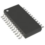 CDC2351QDBG4

The activity of extra discounts on wholesale prices is in full swing…
Please fill in your contact information and we will send you the latest wholesale price list.




