 ChipApex | Global Electronic Components Supplier

SEARCH
Search Product
Search Post
— IC芯片 | 连接器 | 传感器 | 被动器件 —
Search productSearch post
— IC芯片 | 连接器 | 传感器 | 被动器件 —
Consult the customer manager about the wholesale price.
consultation hotline:86-132-6715-2157
email:[email protected]
Contact the product manager for consultation. One-stop consultation is available.
Do you want a lower wholesale price? Please send us your inquiry and we will reply immediately.
The CDC2351QDBR is an automotive-grade clock buffer manufactured by Texas Instruments. It features a single circuit with a 1:10 input-to-output ratio, distributing one LVTTL input signal to ten LVTTL tri-state outputs. The device operates within a supply voltage range of 3V to 3.6V and supports maximum frequencies up to 100 MHz. Designed for robust performance in demanding environments, it functions across an extended operating temperature range from -40°C to 125°C. The component is housed in a 24-SSOP package (5.30mm width) and is supplied in tape and reel format.
Verify the specific revision level and manufacturing date code upon order confirmation. Confirm that the 24-SSOP footprint matches the target PCB design constraints. Ensure the supply voltage domain strictly adheres to the 3V–3.6V specification to prevent device malfunction or degradation over the specified -40°C to 125°C operational window.
Select this component when an automotive-grade clock buffer with LVTTL compatibility is required. The 1:10 ratio suits applications needing moderate fanout without differential signaling. Compare against the non-automotive CDC351 series if extended temperature ratings or automotive certification are not mandatory for the specific application environment.
This part belongs to the CDC235x family of clock buffers designed for high-reliability applications. The 'Q' designation indicates automotive qualification, while the 'DBR' suffix specifies the 24-SSOP package and tape-and-reel packaging. It serves as a specialized variant within the broader CDC351 product line, tailored for automotive electronics requiring wider thermal tolerance.
The CDC351IDWR is a functional equivalent but lacks automotive qualification and has a lower maximum operating temperature of 85°C. Verify that the reduced thermal rating meets the specific environmental requirements before substituting.
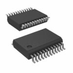 CDC2351QDBR

The activity of extra discounts on wholesale prices is in full swing…
Please fill in your contact information and we will send you the latest wholesale price list.





