 ChipApex | Global Electronic Components Supplier
CDC2510APWR
Search Product
Search Post
— IC芯片 | 连接器 | 传感器 | 被动器件 —
Search productSearch post
— IC芯片 | 连接器 | 传感器 | 被动器件 —
Consult the customer manager about the wholesale price.
consultation hotline:86-132-6715-2157
email:[email protected]
Contact the product manager for consultation. One-stop consultation is available.
Do you want a lower wholesale price? Please send us your inquiry and we will reply immediately.
The CDC2510APWR is a high-performance, low-skew, low-jitter phase-lock loop (PLL) clock driver manufactured by Texas Instruments. It operates at a supply voltage of 3 V to 3.6 V and supports a maximum frequency of 100 MHz. The device distributes one clock input to ten outputs within a single bank using a 24-pin TSSOP package. It features integrated series-damping resistors for point-to-point loads and includes an on-chip PLL loop filter. The component is characterized for operation from 0°C to 70°C.
Verify the current marketing status before procurement as the device may be classified as not recommended for new designs. Confirm the specific ordering suffix matches the required packaging quantity and environmental compliance standards. Ensure the design accounts for the stabilization time required for the PLL to achieve phase lock after power-up or reference signal changes.
Select this component when a fixed-frequency, fixed-phase reference signal is available at the CLK input to ensure proper PLL synchronization. Consider the 1 ms stabilization time requirement during system initialization. Verify that the load capacitance does not exceed the specified limits for accurate timing performance. Evaluate the NRND status if designing a long-term production system.
The CDC2510A belongs to the 2510 series of PLL clock drivers designed for synchronous memory interfaces. It shares functional similarities with other devices in the family but is specifically optimized for distributing a single clock source to multiple synchronous DRAM banks. The 'PWR' suffix indicates the plastic TSSOP package variant.
The datasheet explicitly recommends using the CDCVF2510A as a replacement for this device.
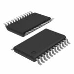 CDC2510APWR
The activity of extra discounts on wholesale prices is in full swing…
Please fill in your contact information and we will send you the latest wholesale price list.





