 ChipApex | Global Electronic Components Supplier
CDC2510BPWR
Search Product
Search Post
— IC芯片 | 连接器 | 传感器 | 被动器件 —
Search productSearch post
— IC芯片 | 连接器 | 传感器 | 被动器件 —
Consult the customer manager about the wholesale price.
consultation hotline:86-132-6715-2157
email:[email protected]
Contact the product manager for consultation. One-stop consultation is available.
Do you want a lower wholesale price? Please send us your inquiry and we will reply immediately.
The CDC2510BPWR is a 3.3-V phase-lock loop (PLL) clock driver designed for synchronous DRAM applications. It distributes one clock input to ten outputs with low skew and jitter. Operating frequencies range from 25 MHz to 125 MHz, with a supply voltage of 3 V to 3.6 V. The device features integrated series damping resistors and requires no external RC network. It operates within a temperature range of 0°C to 70°C in a 24-pin TSSOP package.
Verify the specific ordering suffix 'B' against the manufacturer's current documentation to confirm availability and exact electrical tolerances. Confirm that the 24-TSSOP package dimensions match the target PCB footprint requirements before finalizing procurement orders.
Select this component when a single reference clock must be distributed to multiple synchronous memory banks with minimal skew. Ensure the application supports the required stabilization time for the internal PLL to achieve phase lock after power-up or signal changes.
This part belongs to the Texas Instruments CDC2510 family of PLL clock drivers. The 'B' suffix typically denotes a specific revision or performance grade within the product line, while 'PWR' indicates the plastic small-outline package type with tape-and-reel packaging.
Check for CDC2510CPWR or CDC2510PWG4 as potential alternatives. Verify pin compatibility and operating temperature ranges before substitution.
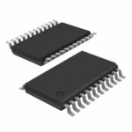 CDC2510BPWR
The activity of extra discounts on wholesale prices is in full swing…
Please fill in your contact information and we will send you the latest wholesale price list.





