 ChipApex | Global Electronic Components Supplier
CDC2510CPWG4
Search Product
Search Post
— IC芯片 | 连接器 | 传感器 | 被动器件 —
Search productSearch post
— IC芯片 | 连接器 | 传感器 | 被动器件 —
Consult the customer manager about the wholesale price.
consultation hotline:86-132-6715-2157
email:[email protected]
Contact the product manager for consultation. One-stop consultation is available.
Do you want a lower wholesale price? Please send us your inquiry and we will reply immediately.
The CDC2510CPWG4 is a Phase-Lock Loop (PLL) clock driver manufactured by Texas Instruments. It operates within a supply voltage range of 3 V to 3.6 V and supports a maximum frequency of 125 MHz. The device features a single circuit configuration with a 1:10 input-to-output ratio, providing ten output channels for clock distribution. It is housed in a 24-TSSOP package with a width of 4.40 mm. The component is designed for surface-mount installation and functions reliably across an operating temperature range from 0°C to +85°C.
Verify the specific suffix 'CPW' against official datasheets to confirm the commercial temperature grade and packaging variant. Ensure the G4 designation aligns with current RoHS compliance requirements. Cross-reference the manufacturer part number directly with the original equipment manufacturer's database to validate authenticity and traceability before procurement.
Select this component when a 125 MHz PLL clock driver with ten outputs is required. Confirm that the 3V to 3.6V supply voltage matches the system power rails. Verify that the 24-TSSOP package dimensions fit the available PCB footprint. Ensure the commercial temperature range meets the environmental constraints of the target application.
This part belongs to the CDC2510 family of PLL clock drivers. It shares functional similarities with variants such as the CDC2510PWR but differs in package type and temperature rating. The family is designed for applications requiring robust clock distribution with minimal jitter. Other members may offer different output counts or voltage ranges.
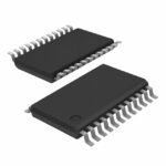 CDC2510CPWG4
The activity of extra discounts on wholesale prices is in full swing…
Please fill in your contact information and we will send you the latest wholesale price list.





