 ChipApex | Global Electronic Components Supplier

SEARCH
Search Product
Search Post
— IC芯片 | 连接器 | 传感器 | 被动器件 —
Search productSearch post
— IC芯片 | 连接器 | 传感器 | 被动器件 —
Consult the customer manager about the wholesale price.
consultation hotline:86-132-6715-2157
email:[email protected]
Contact the product manager for consultation. One-stop consultation is available.
Do you want a lower wholesale price? Please send us your inquiry and we will reply immediately.
The CDC318ADLG4 is a clock buffer and distribution IC manufactured by Texas Instruments. It functions as a 1-to-18 fanout buffer, accepting an LVTTL input signal and providing up to 18 LVTTL or TTL outputs. The device supports a maximum operating frequency of 100 MHz and requires a supply voltage range of 3.135 V to 3.465 V. It is housed in a 48-BSSOP (7.50 mm width) surface-mount package with a tube packaging style. The component operates within a commercial temperature range of 0°C to +70°C.
Verify the specific ordering suffix 'G4' against the manufacturer's current documentation to confirm compliance status and pin compatibility. Ensure the design accommodates the narrow 3.135 V to 3.465 V supply voltage window. Confirm that the 48-SSOP package dimensions fit the target PCB footprint constraints.
Select this component when a single clock source must drive multiple LVTTL/TTL destinations without buffering amplification. The fixed 1:18 ratio limits flexibility compared to programmable drivers. Verify that the system power supply can maintain stability within the specified 3.135 V to 3.465 V range to ensure correct logic threshold operation.
This part belongs to the Texas Instruments clock buffer family. It serves as a passive distribution element rather than a programmable synthesizer. The 'G4' suffix typically indicates lead-free manufacturing compliance, though verification with official datasheets is required. It complements active clock generators by handling load distribution.
Direct replacements must match the 1:18 ratio, 48-SSOP package, and LVTTL/TTL I/O levels. Check for equivalent parts from other manufacturers offering identical pinouts and electrical specifications. Verify if alternative packages like SOIC are available if board space allows.
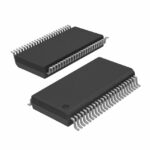 CDC318ADLG4

The activity of extra discounts on wholesale prices is in full swing…
Please fill in your contact information and we will send you the latest wholesale price list.






