 ChipApex | Global Electronic Components Supplier

SEARCH
Search Product
Search Post
— IC芯片 | 连接器 | 传感器 | 被动器件 —
Search productSearch post
— IC芯片 | 连接器 | 传感器 | 被动器件 —
Consult the customer manager about the wholesale price.
consultation hotline:86-132-6715-2157
email:[email protected]
Contact the product manager for consultation. One-stop consultation is available.
Do you want a lower wholesale price? Please send us your inquiry and we will reply immediately.
The CDC318ADLR is a clock buffer and driver manufactured by Texas Instruments, designed to distribute a single input clock signal to eighteen output lines. It operates within a supply voltage range of 3.135V to 3.465V and supports a maximum frequency of 100 MHz. The device accepts LVTTL inputs and provides LVTTL or TTL outputs. It is housed in a 48-SSOP package with dimensions of 7.50mm width and is rated for an operating temperature range of 0°C to 70°C.
Verify the specific ordering suffix against the manufacturer's official documentation to confirm package type and reel specifications. Ensure the selected variant matches the required tape and reel or cut tape packaging format for automated assembly processes.
Select this component when a single clock source must drive up to eighteen loads simultaneously. Confirm that the system logic levels align with the LVTTL input and LVTTL/TTL output capabilities. Verify that the 48-pin SSOP footprint fits the available PCB space and that the 0°C to 70°C temperature range meets the environmental requirements.
This part belongs to the CDC318 family of clock drivers from Texas Instruments. These devices are engineered for high-speed clock distribution applications where signal integrity and low skew are critical. The family typically includes variants with different pin counts and control interfaces to suit various system architectures.
Check for direct replacements within the CDC318 series or other 1:18 clock buffers from Texas Instruments. Ensure any substitute maintains the same 48-SSOP package, 100 MHz frequency rating, and LVTTL/TTL electrical characteristics.
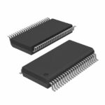 CDC318ADLR

The activity of extra discounts on wholesale prices is in full swing…
Please fill in your contact information and we will send you the latest wholesale price list.






