 ChipApex | Global Electronic Components Supplier

SEARCH
Search Product
Search Post
— IC芯片 | 连接器 | 传感器 | 被动器件 —
Search productSearch post
— IC芯片 | 连接器 | 传感器 | 被动器件 —
Consult the customer manager about the wholesale price.
consultation hotline:86-132-6715-2157
email:[email protected]
Contact the product manager for consultation. One-stop consultation is available.
Do you want a lower wholesale price? Please send us your inquiry and we will reply immediately.
The CDC351DB is a single-circuit fanout buffer manufactured by Texas Instruments, designed for clock distribution applications. It provides a 1:10 input-to-output ratio with LVTTL-compatible inputs and outputs that support tri-state functionality. The device operates within a supply voltage range of 3V to 3.6V and supports maximum frequencies up to 100 MHz. Packaged in a 24-SSOP (5.30mm width) surface-mount case, it is rated for commercial operating temperatures between 0°C and 70°C.
Verify the package type against project requirements, as this specific part number utilizes a 24-SSOP tube packaging format. Confirm that the commercial temperature range of 0°C to 70°C meets the environmental specifications for the intended deployment scenario before finalizing procurement decisions.
Select the CDC351DB when a single-input, ten-output buffer is required for LVTTL clock signals. Ensure the design environment remains within the 0°C to 70°C operational limit. For industrial temperature ranges or differential signaling requirements, alternative models such as the CDC351IDW series should be evaluated instead.
This component belongs to the Texas Instruments clock buffer family, specifically engineered for low-power clock distribution tasks. It serves as a standard solution for expanding clock signals in consumer electronics and general-purpose digital logic circuits where LVTTL compatibility is essential.
The CDC351IDB offers identical electrical characteristics but extends the operating temperature range to -40°C ~ 85°C. The CDC351IDWR variant provides tape-and-reel packaging for automated assembly processes while maintaining the extended temperature rating.
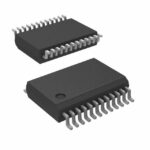 CDC351DB

The activity of extra discounts on wholesale prices is in full swing…
Please fill in your contact information and we will send you the latest wholesale price list.





