 ChipApex | Global Electronic Components Supplier

SEARCH
Search Product
Search Post
— IC芯片 | 连接器 | 传感器 | 被动器件 —
Search productSearch post
— IC芯片 | 连接器 | 传感器 | 被动器件 —
Consult the customer manager about the wholesale price.
consultation hotline:86-132-6715-2157
email:[email protected]
Contact the product manager for consultation. One-stop consultation is available.
Do you want a lower wholesale price? Please send us your inquiry and we will reply immediately.
The CDC351DBR is a single-circuit fanout buffer manufactured by Texas Instruments, designed for clock distribution applications. It provides a 1:10 input-to-output ratio with LVTTL-compatible inputs and tri-state LVTTL outputs. The device supports maximum frequencies of 100 MHz and operates on a supply voltage range of 3V to 3.6V. Packaged in a 24-SSOP (5.30mm width) case, it is available in tape and reel or cut tape formats. The component functions without differential signaling capabilities and is rated for commercial operating temperatures between 0°C and 70°C.
Verify the package type matches the design requirements, as the DBR suffix indicates a 24-SSOP form factor rather than the SOIC variant. Confirm that the commercial temperature grade (0°C to 70°C) meets the operational environment specifications. Ensure power supply rails remain within the 3V to 3.6V range to maintain signal integrity and proper logic threshold levels during operation.
Select this component when a low-cost, single-ended LVTTL clock driver is required for moderate-speed digital systems. The 100 MHz limit suits standard microprocessor and memory bus clocks. Consider the 24-SSOP package constraints regarding PCB space and thermal dissipation. Verify that the tri-state functionality aligns with system bus control requirements for multiple clock domains.
This part belongs to the broader family of clock buffer and driver integrated circuits from Texas Instruments. It serves as a specific solution for distributing a single clock source to ten downstream loads. The device complements other timing components like oscillators and PLLs by providing signal regeneration and load isolation within digital electronic architectures.
Publicly confirmed substitute part numbers are not available in the provided documentation.
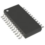 CDC351DBR

The activity of extra discounts on wholesale prices is in full swing…
Please fill in your contact information and we will send you the latest wholesale price list.





