 ChipApex | Global Electronic Components Supplier

SEARCH
Search Product
Search Post
— IC芯片 | 连接器 | 传感器 | 被动器件 —
Search productSearch post
— IC芯片 | 连接器 | 传感器 | 被动器件 —
Consult the customer manager about the wholesale price.
consultation hotline:86-132-6715-2157
email:[email protected]
Contact the product manager for consultation. One-stop consultation is available.
Do you want a lower wholesale price? Please send us your inquiry and we will reply immediately.
The Texas Instruments CDC351DW is a single-circuit fanout buffer designed for clock distribution applications. It accepts one LVTTL input and provides ten tri-state LVTTL outputs, operating at a maximum frequency of 100 MHz. The device functions within a supply voltage range of 3V to 3.6V and is rated for an industrial temperature range of 0°C to 70°C. Packaged in a 24-SOIC surface-mount case with a 7.50mm width, it serves as a dedicated clock driver for digital systems requiring signal splitting without differential signaling capabilities.
Verify the package type matches the required bulk or tube format during ordering. Confirm that the 0°C to 70°C commercial temperature rating meets the operational environment requirements. Ensure the 24-SOIC footprint aligns with the PCB layout specifications before procurement.
Select this component when a single-ended LVTTL clock source must drive up to ten loads simultaneously. The tri-state feature allows for dynamic control of the clock signals. Verify that the system voltage remains strictly between 3V and 3.6V to ensure proper logic level compatibility and device functionality.
This part belongs to the Texas Instruments clock buffer family, specifically engineered for distributing timing signals. The CDC351DW variant utilizes a standard SOIC package suitable for automated surface-mount assembly processes, distinguishing it from through-hole or smaller footprint alternatives in the same series.
Check for pin-compatible alternatives such as the CDC351IDBR or CDC351IDW if extended temperature ranges or tape-and-reel packaging are required. Ensure any substitute maintains the 1:10 ratio and LVTTL interface specifications.
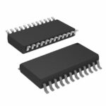 CDC351DW

The activity of extra discounts on wholesale prices is in full swing…
Please fill in your contact information and we will send you the latest wholesale price list.






