 ChipApex | Global Electronic Components Supplier

SEARCH
Search Product
Search Post
— IC芯片 | 连接器 | 传感器 | 被动器件 —
Search productSearch post
— IC芯片 | 连接器 | 传感器 | 被动器件 —
Consult the customer manager about the wholesale price.
consultation hotline:86-132-6715-2157
email:[email protected]
Contact the product manager for consultation. One-stop consultation is available.
Do you want a lower wholesale price? Please send us your inquiry and we will reply immediately.
The CDC351IDBR is a single-circuit fanout buffer manufactured by Texas Instruments, designed for clock distribution applications. It provides a 1:10 input-to-output ratio with LVTTL inputs and LVTTL tri-state outputs. The device supports maximum frequencies of 100 MHz and operates on a supply voltage range of 3V to 3.6V. Packaged in a 24-SSOP (0.209 inch width) format within a tape and reel configuration, it functions reliably across an industrial temperature range of -40°C to +85°C.
Verify the package type matches the required 24-SSOP form factor. Confirm that the 100 MHz frequency limit meets system requirements. Ensure the 3V to 3.6V supply voltage aligns with the target power rails. Check the -40°C to +85°C operating temperature range against environmental conditions.
Select this component when a single-input, ten-output clock buffer is needed. The LVTTL interface compatibility is suitable for standard logic families. The tri-state output feature allows for bus sharing or controlled signal gating. Verify pin compatibility if replacing older variants like the IDW tube version.
This part belongs to the Texas Instruments clock buffer family. It serves as a low-skew driver for distributing clock signals across multiple loads. The TR suffix indicates tape and reel packaging, optimized for automated surface-mount assembly processes.
The CDC351IDW is a compatible alternative in tube packaging. Both share identical electrical specifications and pinouts. Verify that the manufacturing lot date codes meet project timelines.
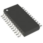 CDC351IDBR

The activity of extra discounts on wholesale prices is in full swing…
Please fill in your contact information and we will send you the latest wholesale price list.





