 ChipApex | Global Electronic Components Supplier

SEARCH
Search Product
Search Post
— IC芯片 | 连接器 | 传感器 | 被动器件 —
Search productSearch post
— IC芯片 | 连接器 | 传感器 | 被动器件 —
Consult the customer manager about the wholesale price.
consultation hotline:86-132-6715-2157
email:[email protected]
Contact the product manager for consultation. One-stop consultation is available.
Do you want a lower wholesale price? Please send us your inquiry and we will reply immediately.
The CDC3RL02BYFPR is a dual-channel clock buffer manufactured by Texas Instruments, designed for square or sine-to-square wave conversion. It operates within a supply voltage range of 2.3 V to 5.5 V and supports maximum input frequencies up to 100 MHz, with a maximum output frequency of 52 MHz. The device features a propagation delay of 11 ns and accepts both sine and square wave inputs, producing square wave outputs. Packaged in an 8-DSBGA format, it functions reliably across an operating temperature range of -40°C to +85°C.
Verify the specific ordering suffix BYFPR against the manufacturer's official datasheet to confirm package type and tape/reel specifications. Ensure compatibility with the required 8-DSBGA footprint during PCB layout. Confirm that the 2.3 V to 5.5 V supply range aligns with the target system power rails before procurement.
Select this component when a dual-channel buffer capable of handling sine inputs is required. The 52 MHz maximum output frequency limits its use in high-speed digital designs compared to GHz-range buffers. Verify that the 11 ns propagation delay meets the timing constraints of the application. The wide supply voltage range allows flexibility in systems using 3.3 V or 5 V logic levels.
This part belongs to the CDC3RL02 series of clock buffers. It serves as a signal conditioning element for converting oscillatory signals into clean square waves for digital processing. The DSBGA package offers a small form factor for space-constrained designs.
Check for direct pin-compatible alternatives within the same Texas Instruments family that offer higher speed or different packaging options if the current specifications do not fully meet design requirements.
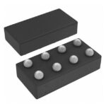 CDC3RL02BYFPR

The activity of extra discounts on wholesale prices is in full swing…
Please fill in your contact information and we will send you the latest wholesale price list.





