 ChipApex | Global Electronic Components Supplier

SEARCH
Search Product
Search Post
— IC芯片 | 连接器 | 传感器 | 被动器件 —
Search productSearch post
— IC芯片 | 连接器 | 传感器 | 被动器件 —
Consult the customer manager about the wholesale price.
consultation hotline:86-132-6715-2157
email:[email protected]
Contact the product manager for consultation. One-stop consultation is available.
Do you want a lower wholesale price? Please send us your inquiry and we will reply immediately.
The CDC3RL02YFPR is a single-channel fanout buffer manufactured by Texas Instruments, designed for clock distribution applications. It accepts LVCMOS inputs and provides LVCMOS outputs with a 1:2 splitting ratio. The device supports a maximum operating frequency of 52 MHz and functions within a supply voltage range of 2.3 V to 5.5 V. Packaged in an 8-DSBGA (XFBGA) surface-mount case, it operates reliably across an industrial temperature range of -40°C to +85°C. This component serves as a low-skew buffer for distributing clock signals in digital systems.
Verify the specific ordering suffix against the manufacturer's official documentation to ensure correct package type and reel specifications. Confirm that the 8-DSBGA package variant matches the design requirements for footprint and thermal management. Cross-reference the part number with the latest datasheet to validate electrical parameters and availability status before finalizing procurement plans.
Select this component when a single-ended LVCMOS clock signal requires splitting into two paths with minimal skew. Ensure the system power supply remains within the 2.3 V to 5.5 V range to maintain proper operation. Verify that the 52 MHz frequency limit meets the target application's timing requirements. Consider the 8-DSBGA package constraints for PCB layout and soldering processes during the design phase.
This part belongs to the family of clock buffers and drivers produced by Texas Instruments. It is specifically categorized as a fanout buffer intended for signal distribution rather than generation or multiplication. The DSBGA package offers a compact form factor suitable for space-constrained electronic designs requiring reliable clock signal integrity.
Consult the manufacturer's replacement guide for verified alternative part numbers. Ensure any substitute maintains compatible LVCMOS levels, similar frequency capabilities, and identical package dimensions to avoid redesign efforts.
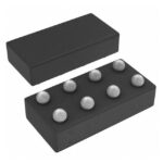 CDC3RL02YFPR

The activity of extra discounts on wholesale prices is in full swing…
Please fill in your contact information and we will send you the latest wholesale price list.




