 ChipApex | Global Electronic Components Supplier
CDC516DGG
Search Product
Search Post
— IC芯片 | 连接器 | 传感器 | 被动器件 —
Search productSearch post
— IC芯片 | 连接器 | 传感器 | 被动器件 —
Consult the customer manager about the wholesale price.
consultation hotline:86-132-6715-2157
email:[email protected]
Contact the product manager for consultation. One-stop consultation is available.
Do you want a lower wholesale price? Please send us your inquiry and we will reply immediately.
The CDC516DGG is a clock driver manufactured by Texas Instruments, belonging to the CDC516 series. It operates within a supply voltage range of 3 V to 3.6 V and supports a maximum output frequency of 400 MHz. The device features multiple multiplication and division factors, including 1:2, 1:4, 1:5, 1:6, 1:8, 1:10, and 1:5, 1:4 configurations. It utilizes LVCMOS, LVTTL, LVECL, LVPECL, SSTL-18, and SSTL-2 output types with corresponding input types such as Clock, CMOS, TTL, Differential, LVCMOS, SSTL-18, and SSTL-2. The component is housed in a TSSOP-48 package and functions reliably across an operating temperature range from -40°C to +85°C.
Verify the specific suffix and revision level against the manufacturer's current datasheet to ensure compatibility with design requirements. Confirm packaging details and environmental compliance status prior to ordering. Cross-reference part numbers with authorized distributors to avoid counterfeit components. Check for any recent lifecycle notices or obsolescence warnings associated with this specific model variant.
Select this component when a wide variety of output voltage standards and programmable frequency scaling are required. Ensure the system power supply aligns with the 3 V to 3.6 V operational window. Verify that the thermal environment remains within the specified -40°C to +85°C range. Consider the TSSOP-48 footprint constraints during PCB layout planning to maintain signal integrity at high frequencies.
The CDC516DGG is part of Texas Instruments' broader CDC516 family of clock drivers designed for complex timing architectures. This series provides versatile solutions for generating and distributing clock signals in systems requiring precise synchronization. The DGG suffix specifically denotes the TSSOP-48 surface-mount package, distinguishing it from other physical form factors available within the same functional family.
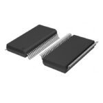 CDC516DGG
The activity of extra discounts on wholesale prices is in full swing…
Please fill in your contact information and we will send you the latest wholesale price list.






