 ChipApex | Global Electronic Components Supplier
CDC536DB
Search Product
Search Post
— IC芯片 | 连接器 | 传感器 | 被动器件 —
Search productSearch post
— IC芯片 | 连接器 | 传感器 | 被动器件 —
Consult the customer manager about the wholesale price.
consultation hotline:86-132-6715-2157
email:[email protected]
Contact the product manager for consultation. One-stop consultation is available.
Do you want a lower wholesale price? Please send us your inquiry and we will reply immediately.
The CDC536DB is a PLL clock driver IC manufactured by Texas Instruments, housed in a 28-SSOP package. It operates within a supply voltage range of 3V to 3.6V and supports a maximum frequency of 100MHz. The device features one circuit with a 1:6 input-to-output ratio, utilizing TTL inputs and LVTTL outputs. It includes integrated divider and multiplier functions for frequency synthesis. The component is designed for surface mount installation and functions reliably across an operating temperature range of 0°C to 70°C.
Verify the current lifecycle status before procurement as availability may vary. Confirm that the 28-SSOP package dimensions align with the target PCB footprint. Ensure the 3V to 3.6V supply voltage range matches the system power architecture. Validate that the 100MHz maximum frequency meets the design requirements. Check for RoHS compliance if environmental regulations apply to the final assembly.
Select this component when a single-channel PLL clock driver with frequency multiplication and division is required. The 28-SSOP package suits applications with limited board space. Ensure the system operates within the specified 0°C to 70°C temperature range. Verify that TTL input and LVTTL output levels are compatible with connected logic devices. Consider the 1:6 output ratio when designing the clock tree structure.
The CDC536DB belongs to the CDC536 family of clock drivers from Texas Instruments. This series focuses on providing robust clock signal management with integrated PLL functionality. The device serves as a key component in timing circuits where frequency synthesis and distribution are critical. It complements other clock generators and synthesizers in complex digital systems.
The CDC536DBG4 is listed as a manufacturer-recommended substitute. Verify pinout and electrical specifications match before substitution. Ensure the replacement part meets the same package and thermal requirements.
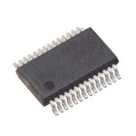 CDC536DB
The activity of extra discounts on wholesale prices is in full swing…
Please fill in your contact information and we will send you the latest wholesale price list.







