 ChipApex | Global Electronic Components Supplier
CDC536DBG4
Search Product
Search Post
— IC芯片 | 连接器 | 传感器 | 被动器件 —
Search productSearch post
— IC芯片 | 连接器 | 传感器 | 被动器件 —
Consult the customer manager about the wholesale price.
consultation hotline:86-132-6715-2157
email:[email protected]
Contact the product manager for consultation. One-stop consultation is available.
Do you want a lower wholesale price? Please send us your inquiry and we will reply immediately.
The CDC536DBG4 is a PLL clock driver IC manufactured by Texas Instruments, housed in a 28-SSOP package. It operates within a supply voltage range of 3V to 3.6V and supports frequencies up to 100MHz. The device features one circuit with a 1:6 input-to-output ratio, utilizing TTL inputs and LVTTL outputs. It includes frequency division and multiplication capabilities without differential signaling. The component functions within an operating temperature range of 0°C to 70°C and complies with RoHS3 standards.
Verify the current availability status as this specific part number may be discontinued or subject to change. Confirm that the replacement package type matches the required footprint. Ensure compliance with environmental regulations such as RoHS3 before finalizing procurement decisions for production runs.
Select this component when a single-channel PLL clock driver with 1:6 fan-out is required. Ensure the design accommodates the 3V to 3.6V supply voltage constraint. Verify that the 28-SSOP package dimensions fit the board layout constraints and thermal requirements for the intended operating temperature range.
This device belongs to the CDC536 family of clock drivers from Texas Instruments. It shares core specifications with variants like CDC536DB but differs in packaging suffixes. The family is designed for applications needing reliable clock generation with integrated frequency control capabilities in a compact surface-mount form factor.
The CDC536DB is listed as a manufacturer-recommended substitute. Verify pin compatibility and electrical parameters before substitution. Ensure the alternative package variant meets the same mechanical and thermal requirements as the original design.
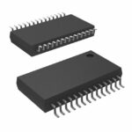 CDC536DBG4
The activity of extra discounts on wholesale prices is in full swing…
Please fill in your contact information and we will send you the latest wholesale price list.





