 ChipApex | Global Electronic Components Supplier
CDC5801ADBQ
Search Product
Search Post
— IC芯片 | 连接器 | 传感器 | 被动器件 —
Search productSearch post
— IC芯片 | 连接器 | 传感器 | 被动器件 —
Consult the customer manager about the wholesale price.
consultation hotline:86-132-6715-2157
email:[email protected]
Contact the product manager for consultation. One-stop consultation is available.
Do you want a lower wholesale price? Please send us your inquiry and we will reply immediately.
The CDC5801ADBQ is a low jitter PLL-based multiplier and divider manufactured by Texas Instruments. It operates as a zero delay PLL clock multiplier with one circuit. The device supports an input frequency range from 12.5 MHz to 240 MHz, producing output frequencies up to 280 MHz. It functions within a supply voltage range of 3 V to 3.6 V, typically at 3.3 V. The component utilizes Silicon technology and is housed in a QSOP-24 package for surface mount installation. It accepts HSTL, LVPECL, or LVTTL input levels and provides LVDS, LVPECL, or LVTTL output levels. The operational temperature range spans from -40°C to +85°C.
Verify the specific ordering suffix to confirm package type and tape/reel versus tube packaging. Confirm RoHS compliance status through official manufacturer documentation before procurement. Ensure the supplier source is authorized to guarantee component authenticity and traceability. Check for moisture sensitivity level requirements during storage and handling procedures.
Select this component when a single-channel zero-delay PLL is required for clock multiplication or division. Verify that the system input frequency falls within the 12.5 MHz to 240 MHz range. Ensure the target output frequency does not exceed 280 MHz. Confirm that the QSOP-24 package footprint is compatible with the PCB layout design.
This part belongs to the CDC5801A series of low jitter PLLs. It is designed for applications demanding precise clock edge alignment. The device integrates a voltage-controlled oscillator and feedback loop to minimize phase error between input and output clocks.
Consult official substitution guides for equivalent devices. Verify pin compatibility and electrical specifications before replacing.
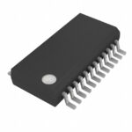 CDC5801ADBQ
The activity of extra discounts on wholesale prices is in full swing…
Please fill in your contact information and we will send you the latest wholesale price list.






