 ChipApex | Global Electronic Components Supplier
CDC5801DBQR
Search Product
Search Post
— IC芯片 | 连接器 | 传感器 | 被动器件 —
Search productSearch post
— IC芯片 | 连接器 | 传感器 | 被动器件 —
Consult the customer manager about the wholesale price.
consultation hotline:86-132-6715-2157
email:[email protected]
Contact the product manager for consultation. One-stop consultation is available.
Do you want a lower wholesale price? Please send us your inquiry and we will reply immediately.
The CDC5801DBQR is a low jitter clock multiplier and divider manufactured by Texas Instruments. It accepts a single-ended reference clock input ranging from 19 MHz to 125 MHz and generates differential outputs (CLKOUT/CLKOUTB) with frequencies between 12.5 MHz and 500 MHz. The device supports multiplication ratios of x4, x6, or x8, and division ratios of /2, /3, or /4. It features programmable bidirectional delay steps of 2.6 mUI for phase alignment. Typical phase jitter is 8.0 ps (12 kHz to 20 MHz) at 500 MHz, with typical RMS period jitter of 2.1 ps. Operating voltage ranges from 3.0 V to 3.6 V, with typical power consumption of 200 mW at 500 MHz. It is packaged in a shrink small-outline package (DBQ).
Verify the specific ordering suffix 'R' indicates tape-and-reel packaging when sourcing this component. Confirm that the DBQ package type matches the target board layout requirements. Ensure the operating temperature range of -40°C to 85°C aligns with the system environment specifications before finalizing procurement decisions.
Select this component when low jitter performance is critical for high-speed digital interfaces. The CDC5801 is suitable for applications requiring flexible frequency synthesis from a single reference source. Consider the programmable delay feature if strict phase alignment between reference and output clocks is necessary for system synchronization.
The CDC5801 belongs to Texas Instruments' family of low jitter clock multipliers and dividers. It is designed to replace discrete clock generation solutions by integrating PLL, phase aligner, and output drivers into a single compact package. This integration reduces board space and simplifies design complexity for high-performance timing applications.
Public confirmed substitute part numbers are not available in the provided documentation.
The device uses a phase aligner that allows users to delay or advance the CLKOUT/CLKOUTB signals relative to REFCLK in steps of 2.6 mUI using the DLYCTRL and LEADLAG terminals.
The REFCLK terminal accepts LVCMOS and LVTTL inputs directly. Other single-ended signal levels can be supported by programming the proper VDDREF voltage level.
Yes, in Test Mode (P0=1, P1=1, P2=0), both the PLL and phase aligner are bypassed, channeling the REFCLK directly to the CLKOUT/CLKOUTB terminals.
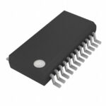 CDC5801DBQR
The activity of extra discounts on wholesale prices is in full swing…
Please fill in your contact information and we will send you the latest wholesale price list.






